Next: 5. Simulation Studies Up: 4. Physical Models Previous: 4.5 Spontaneous and Piezoelectric Contents
The small-signal response of a two-port network
(Fig. 4.21) can be described by several equivalent
parameter sets. The
![]() -matrix (admittance matrix) gives the
relation between input voltages and output currents:
-matrix (admittance matrix) gives the
relation between input voltages and output currents:
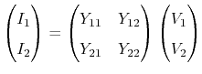 |
(4.82) |
 |
 |
(4.83) | ||
 |
 |
(4.84) |
Another established relation is the
![]() -matrix (impedance
parameters), which links the output voltages to the input currents:
-matrix (impedance
parameters), which links the output voltages to the input currents:
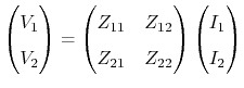 |
(4.85) |
 |
 |
(4.86) | ||
 |
 |
(4.87) |
However, measurement of those parameter sets requires open or shortcut
conditions, which are difficult to achieve at high frequencies. To avoid this
problem, matched loads can be used. Thus, the device is embedded into a
transmission line with a specific impedance (![]() ). For a traveling wave, the
inserted network acts as an impedance, different from the characteristic
impedance of the line. S-parameters are the complex valued reflexion and transmission
coefficients (Fig. 4.22):
). For a traveling wave, the
inserted network acts as an impedance, different from the characteristic
impedance of the line. S-parameters are the complex valued reflexion and transmission
coefficients (Fig. 4.22):
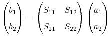 |
(4.88) |
 |
 |
(4.89) | ||
 |
 |
(4.90) |
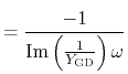
In order to obtain important figures of merit for the frequency characteristics of the devices, such as the cut-off frequency and the maximum oscillation frequency, an equivalent circuit is useful. Here, the one used by Dambrine et al. [363] for FETs is applied (Fig. 4.23). The expressions to calculate the values of its circuit elements are as following [363,364]:
| (4.91) |
| (4.92) | ||
| (4.93) | ||
| (4.94) | ||
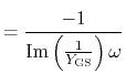
| (4.95) | ||
 |
(4.96) | |
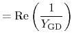
 |
(4.97) | |
 |
(4.98) | |
 |
(4.99) | |
 |
(4.100) | |
 |
(4.101) |
![\includegraphics[width=12cm]{figures/sim/Spara/2Port.eps}](img557.png)
![\includegraphics[width=12cm]{figures/sim/Spara/2PortS.eps}](img568.png)
![\includegraphics[width=15cm]{figures/sim/Spara/EST3.eps}](img579.png)
![\includegraphics[width=13cm]{figures/sim/Spara/Ext.eps}](img604.png)