To examine the influence of clustering effects and field coupling, we
analyzed the p-channel transistor of a  ,
,  CMOS process.
The influence is judged upon the change in the subthreshold characteristics
of the transistor.
CMOS process.
The influence is judged upon the change in the subthreshold characteristics
of the transistor.
We used a p-type substrate ( phosphorus), a
  Å
gate oxide and a heavily doped n-type polysilicon gate. As we applied an
Å
gate oxide and a heavily doped n-type polysilicon gate. As we applied an
 -polysilicon gate the threshold voltage could not be ideally adjusted
by the substrate doping. For threshold adjust we implanted
-polysilicon gate the threshold voltage could not be ideally adjusted
by the substrate doping. For threshold adjust we implanted
 boron with
  , and annealed for
  at
at
 , to form a compensating layer. For source/drain formation we
created a `lighter' doped region implanting
, to form a compensating layer. For source/drain formation we
created a `lighter' doped region implanting 
 at
at
 and, offset by a
  Å sidewall spacer, a `heavier' doped
region by implanting
Å sidewall spacer, a `heavier' doped
region by implanting  at . The subsequent
thermal treatments are approximated by an anneal at for
at . The subsequent
thermal treatments are approximated by an anneal at for  .
.
We simulated this process using PROMIS' analytical ion implantation module for the implantation steps, and the diffusion models DIFN, DIFC and DIFSCL for the annealing steps.
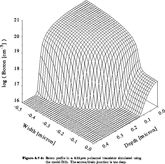
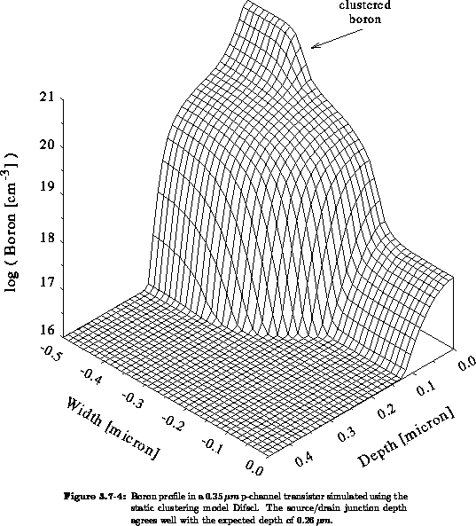
Figures 3.7-3 and 3.7-4 show the final boron
concentration calculated with the diffusion models DIFN and
DIFSCL, respectively. The application of models DIFN and
DIFC produced almost identical boron profiles. The source/drain
junction depth of  is conspicuously deep. From an actually built
device [Maz92] with comparable process conditions the junction depth is
expected to be approximately
is conspicuously deep. From an actually built
device [Maz92] with comparable process conditions the junction depth is
expected to be approximately  . Using the static clustering
model DIFSCL we immediately perceive the clustered peak in the boron
profile in Figure 3.7-4. The source/drain junction depth of
. Using the static clustering
model DIFSCL we immediately perceive the clustered peak in the boron
profile in Figure 3.7-4. The source/drain junction depth of
 meets our expectations.
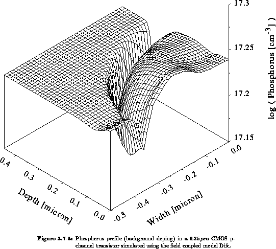
Although the boron profiles simulated with and without field coupling hardly differ, the distortion in the phosphorus profile (from substrate doping) considering field coupling (DIFC) cannot escape notice (Figure 3.7-5).
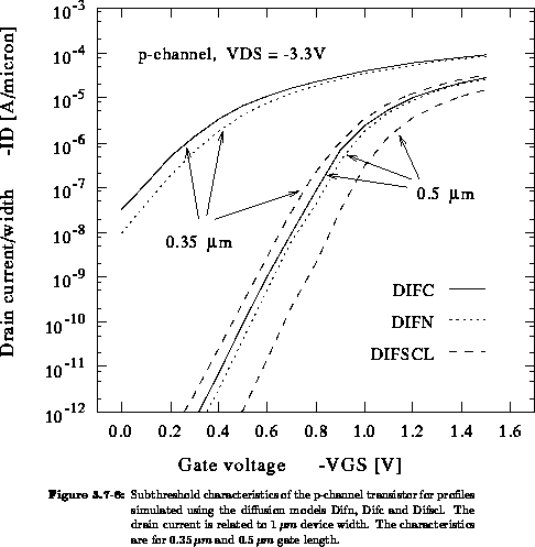
To discover the consequences of applying the (in-)appropriate diffusion
model we calculated the subthreshold characteristics for a and
a  transistor when using the three doping profiles (calculated
from model DIFN, DIFC and DIFSCL). The
subthreshold characteristics were calculated with MINIMOS
[Sel90] including avalanche generation. Since the profiles calculated
by the DIFN and DIFC models extend too far underneath the
gate, the device does not even work for these (wrong)
profiles, as expected, because of punch-through (Figure 3.7-6).
The effect of the too wide profiles is less pronounced for the
device, however, still remarkable. In Figure 3.7-6 the drain
current is divided by the device width in microns. We particularly want to
emphasize that these results (
transistor when using the three doping profiles (calculated
from model DIFN, DIFC and DIFSCL). The
subthreshold characteristics were calculated with MINIMOS
[Sel90] including avalanche generation. Since the profiles calculated
by the DIFN and DIFC models extend too far underneath the
gate, the device does not even work for these (wrong)
profiles, as expected, because of punch-through (Figure 3.7-6).
The effect of the too wide profiles is less pronounced for the
device, however, still remarkable. In Figure 3.7-6 the drain
current is divided by the device width in microns. We particularly want to
emphasize that these results ( junction actually
vs. simulated ) were obtained without any calibration.
junction actually
vs. simulated ) were obtained without any calibration.