Among all technologies photolithography holds the leading position
in pattern transfer in today's semiconductor industry.
The reduction of the lithographic feature sizes towards or even beyond
the used wavelength and the increasing nonplanarity of the
devices place considerable demands onto the lithography process.
The large cost and time necessary for experiments
make simulation an important and especially
cost-effective tool for further improvements.
However, a rigorous description of the
fundamental physical effects governing sub-micrometer-photolithography
places considerable demands onto the modeling, whereby a
three-dimensional simulation becomes necessary.
As a consequence the needed computational resources are extremely
high. In three dimensions some approaches
(e.g.
[1]
[2]
[3])
are suited only for supercomputers, others are already proposed for
workstation based simulation
(e.g.
[4]
[5]
[6]).
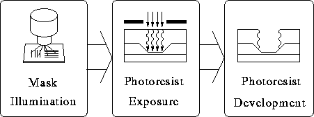
We present an overall three-dimensional photolithography simulator running on modern engineering workstations. The simulator consist of three different modules as shown in Fig. 2, whereby each module accounts for one of the fundamental processes of photolithography: imaging, exposure/bleaching and development.
The lithography simulator calls these three modules sequentially.
As well defined interfaces exist between these modules, they
can be treated independently.
Furthermore, each part requires its specific simulation approach.
The individual tasks and our solutions therefore
are briefly summarized as follows:
The paper is organized according to the simulation flow depicted in Fig. 2. In the next three sections we discuss the imaging, the exposure/bleaching and the development module, respectively. Then we present simulation results for contact hole printing over a planar and a stepped substrate to demonstrate the capability of the simulator. We conclude with a brief summary of the main features of the simulator and the contributions of this paper.