The influence of the nonlinear capacitances can also be formulated as follows: For switching one transistor a total switching charge of
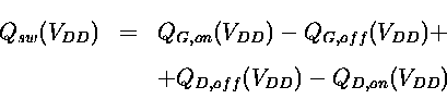 |
(1) |
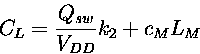
An effective load capacitance CL including interconnects is
then determined as
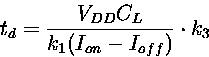
The factors k1 and k2 are used to scale the data of one device
to obtain the delay of a CMOS inverter.
They account for the effective average drive current
((Ion,n-Ioff,n)+(Ion,p-Ioff,p))/2 = k1 (Ion-Ioff) and for the
effective total capacitance (Qsw,n+Qsw,p)/VDD= k2 Qsw/VDD.
Typically, for a CMOS inverter with minimum-size transistors these
factors are k1 = 0.75 and k2 > 2 for NMOS data.
The empirical correction factor k3 is typically < 1
and accounts for the fact that in a circuit the output nodes
start to switch before the input pulse edge is complete.
k3 was determined from device-level simulations of a ring
oscillator with MINIMOS-NT [5] as follows:
setting k1=((Ion,n-Ioff,n)+(Ion,p-Ioff,p))/2(Ion,n-Ioff,n)
and k2=(Qsw,n+Qsw,p)/Qsw,n,
yields k3=td,osc/(k2Qsw/k1(Ion,n-Ioff,n)), where
td,osc is the reference delay time determined from the ring
oscillator. Using the devices of Section 8 k3 was
found to be 0.63.
The value of k3 does not change much with technology.
Evaluating (3) with the same value of k3 for a completely different
technology (an ultra-low-power technology with Vdd=0.2V [6])
using both NMOS and PMOS data gave an error of -22%.
Although (3) and (4) are generally not very accurate,
they reflect the various tendencies very closely and are therefore
well-suited for optimization purposes.
Furthermore, the device characterization method, which is specific to
this approach, can be combined with a more detailed system model
(cf. [7])
to account for the effect of the particular circuit design style
and metalization scheme.
and the loaded-inverter delay is estimated as
![]()
![]()
![]()
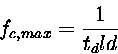
Next: 6 Power Consumption
Up: VLSI Performance Metric Based
Previous: 4 Key Parameters and
G. Schrom, V. De, and S. Selberherr: VLSI Performance Metric Based on Minimum TCAD Simulations
![\begin{figure}
\centerline{\epsfysize=3cm\epsfbox{invckt.eps}
\hspace{6mm}
\epsfysize=5cm\raisebox{6mm}{\rotate[r]{\epsfbox{invmod.eps}}}}\end{figure}](img4.gif)
![\begin{figure}
\centerline{\epsfysize=5.5cm\rotate[r]{\epsfbox{qsw-idea.eps}}
\...
...\epsfysize=3.0cm\raisebox{3mm}{\rotate[r]{\epsfbox{qsw-sim-x.eps}}}}\end{figure}](img6.gif)