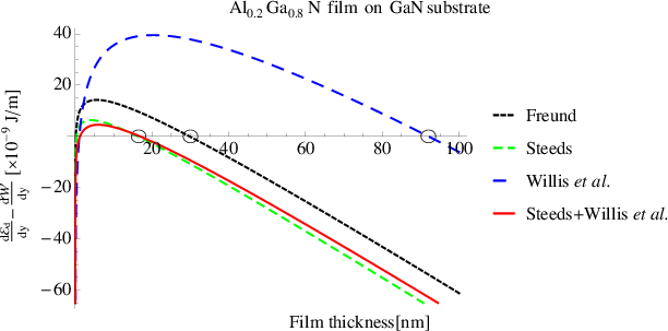
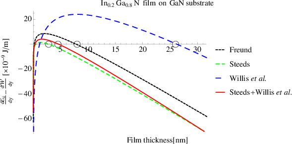
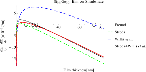
4.5 Overall comparison of various effects on the predicted critical thickness
In order to consider the anisotropy, the difference between the elastic properties of the film
and the substrate as well as the impact of the free surface, the Steeds and the Willis et al.
approaches are combined. Based on the conclusions of Section 4.3, in the following the
contribution of the integral along the core surface S3 is neglected. The detailed
mathematical derivation of this treatment (indicated with Steeds+Willis et al.) is
given in 4.2.3. The model Steeds+Willis et al. is used to compute d d∕dy as a
function of the film thickness for three different alloys: an Al0.2Ga0.8N film on a
GaN substrate, In0.2Ga0.8N on GaN and a Si0.8Ge0.2 film on a Si substrate. The
results are shown and compared with corresponding Freund, Steeds, and Willis et
al. results in Figures 4.11, 4.12, and 4.13. The critical thickness values of the
systems are listed in Table 4.2. Considering all the three systems, the Willis et
al. model increases the critical thickness by ≈ 300% with respect to the Freund
model. The critical thickness value of the theoretically most complete scheme,
Steeds+Willis et al., is always between the Steeds and the Freund values. In particular, the
Steeds+Willis et al. critical thickness is lower by ≈ 50% relative to the Freund critical
thickness for Al0.2Ga0.8N and In0.2Ga0.8N, while it is the same in the case of Si0.8Ge0.2.
d∕dy as a
function of the film thickness for three different alloys: an Al0.2Ga0.8N film on a
GaN substrate, In0.2Ga0.8N on GaN and a Si0.8Ge0.2 film on a Si substrate. The
results are shown and compared with corresponding Freund, Steeds, and Willis et
al. results in Figures 4.11, 4.12, and 4.13. The critical thickness values of the
systems are listed in Table 4.2. Considering all the three systems, the Willis et
al. model increases the critical thickness by ≈ 300% with respect to the Freund
model. The critical thickness value of the theoretically most complete scheme,
Steeds+Willis et al., is always between the Steeds and the Freund values. In particular, the
Steeds+Willis et al. critical thickness is lower by ≈ 50% relative to the Freund critical
thickness for Al0.2Ga0.8N and In0.2Ga0.8N, while it is the same in the case of Si0.8Ge0.2.
| Table 4.2: | Critical thickness values (in nm) of the studied systems. |
|
|
|
|
|
|
|
| | F | F+Ecs | S | S+Ecs | WJB | S+WJB |
|
|
|
|
|
|
|
|
|
|
|
|
|
|
| Al0.2Ga0.8N film on GaN substrate | 30 | 30 | 16 | 12 | 93 | 17 |
|
|
|
|
|
|
|
| In0.2Ga0.8N film on GaN substrate | 8 | 8 | 3 | 0 | 26 | 5 |
|
|
|
|
|
|
|
| Si0.2Ge0.8 film on Si substrate | 18 | 18 | 8 | 6 | 74 | 16 |
|
|
|
|
|
|
|
| |