


Next: 4.6 High-Field Mobility
Up: 4. Mobility Modeling
Previous: 4.4 Bulk Mobility of
Subsections
4.5 Inversion Layer Mobility
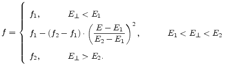
The transport of carriers in the inversion layer is different from that in the
bulk. Carriers in the channel region experience the irregularities at the
Si/SiO interface. The resulting surface mobility is lower than the bulk
mobility, since the carriers in the channel undergo surface roughness
scattering in addition to the bulk scattering mechanisms.
interface. The resulting surface mobility is lower than the bulk
mobility, since the carriers in the channel undergo surface roughness
scattering in addition to the bulk scattering mechanisms.
The electric field component normal to the Si/SiO interface causes the
formation of a potential well which confines carriers to a region close to the
interface to form a two dimensional electron gas (2DEG) or hole gas (2DHG). The
carrier motion is thus quantized in the direction normal to the interface
thereby leading to the formation of sub-bands within the conduction or valence
bands as shown in Fig. 4.5a.
For a (100) surface two sets of sub-bands, the primed and the unprimed subband
ladders, are formed due to the different quantization masses. Within the
triangular well approximation, the energy level of  subband is
inversely proportional to the quantization mass. Therefore, the subbands in the
subband is
inversely proportional to the quantization mass. Therefore, the subbands in the
 valley are less separated in energy, and in absolute values also are
lower in energy than the subbands of
valley are less separated in energy, and in absolute values also are
lower in energy than the subbands of  valleys. The mobility can then
be calculated from the subband structure using numerical methods by taking into
account the scattering rates between the subbands. Such an approach is,
however, quite time intensive and therefore should be replaced by a more
effective analytical modeling approach. Table 4.5 lists a
number of semi-empirical inversion layer mobility models employed in today's
device simulators.
valleys. The mobility can then
be calculated from the subband structure using numerical methods by taking into
account the scattering rates between the subbands. Such an approach is,
however, quite time intensive and therefore should be replaced by a more
effective analytical modeling approach. Table 4.5 lists a
number of semi-empirical inversion layer mobility models employed in today's
device simulators.
| Simulator |
Surface mobility models |
|---|
| |
|
| ATLAS |
Darwish, Lombardi, Shirahata, Shin, Watt, |
| MEDICI |
Mujtaba, Shirahata, Shin, Watt, Darwish |
| DESSIS |
Lombardi/Darwish, Reggiani, |
| MINIMOS-NT |
Selberherr, Lombardi |
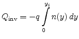
Figure 4.5:
Energy lineups of the conduction subbands in (a) unstrained Si and (b)
Strained Si. Strain changes the lineup of the energies and thus is able to
remove the degeneracy of subband ladders.
Experimental evidences indicate that the inversion layer mobility, when
investigated as a function of the electric field component normal to the
Si/SiO interface, is a function of the doping concentration, the gate and
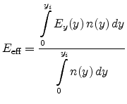
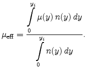
substrate bias and the oxide thickness. The effective mobility, is a spatial
average of the mobility profile in the inversion layer. Sabnis and
Clemens [Sabnis79] demonstrated that that if the effective mobility of
electrons is plotted as a function of the effective transverse electric field
in the inversion layer, the universal mobility curve is obtained.
The effective field for the electrons in the inversion layer is defined as the
average of the normal electric field  experienced by the electrons
weighted by the electron concentration
experienced by the electrons
weighted by the electron concentration  .
.
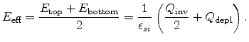
The integration in (4.89) is performed over the depth of the inversion
layer,  . In terms of the field at the top (
 ) and bottom
(
) and bottom
(
 ) of the inversion layer, the effective field becomes
To arrive at (4.90), the relations
derived using Gauss's law are used.
 and
and
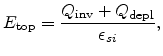
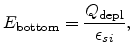
 denote the inversion and depletion charge densities, respectively, and can be
computed as
denote the inversion and depletion charge densities, respectively, and can be
computed as
 |
(4.93) |
 |
(4.94) |
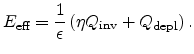
The definition of
 in (4.90) is valid for electrons on
(100) oriented surfaces and can be generalized to
in (4.90) is valid for electrons on
(100) oriented surfaces and can be generalized to
The parameter  is dependent on the orientation of the crystal surface and
can assume values different from
is dependent on the orientation of the crystal surface and
can assume values different from  due to valley repopulation
effects [Lee91]. For estimating the electron mobilities on (110) and (111)
oriented surfaces,
due to valley repopulation
effects [Lee91]. For estimating the electron mobilities on (110) and (111)
oriented surfaces,
 can be assumed.
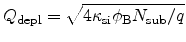
Figure 4.6:
Universal mobility in the Si , inversion layer.
Similar to (4.89) the effective mobility,
 , in Si
inversion layers can be defined as
, in Si
inversion layers can be defined as
Experimentally, the effective mobility can be determined from the drain current
relation (4.24) through
 |
(4.97) |
where
 denotes the drain conductance. The
different regimes of the inversion layer mobility are shown in
Fig. (4.6). At low effective fields, carrier mobility is dominated by
Coulomb scattering, which is more effectively screened at higher effective
fields. At moderate effective fields, phonon scattering determines the
mobility. Finally, in the high-effective field regime, surface roughness
scattering limits the carrier mobility. The universal nature of the carrier
mobility is attributed to the phonon and surface roughness mobilities.
denotes the drain conductance. The
different regimes of the inversion layer mobility are shown in
Fig. (4.6). At low effective fields, carrier mobility is dominated by
Coulomb scattering, which is more effectively screened at higher effective
fields. At moderate effective fields, phonon scattering determines the
mobility. Finally, in the high-effective field regime, surface roughness
scattering limits the carrier mobility. The universal nature of the carrier
mobility is attributed to the phonon and surface roughness mobilities.
The effect of strain on the inversion layer mobility can be understood in terms
of the modification of the subband structure. In the presence of strain, each
subband ladder experiences and additional energy shift as shown in
Fig. 4.5b. Since this shift depends on the valley orientation, it
may be different for each valley and consequently the degeneracy between the
subband ladders can be lifted. Although significant effort has been put by
several groups on the calculation of the mobilities using subband Monte Carlo
techniques [Gamiz02,Roldan96,Fischetti02,Ungersboeck06,Rashed95,Jungemann03b,Fan04],
little work has been done in the area of developing simplified analytical
inversion layer mobility models suitable for device simulations. This is
primarily because of the increased complexity of the physical effects involved
in the inversion layer in the presence of strain.
A semi-empirical modeling approach based on Darwish's mobility
model [Darwish97] for epitaxially grown Si on relaxed SiGe was suggested
by [Roldan03]. The effect of strain was incorporated in the model
through two functions  and
and  , where x denotes the mole
fraction of Ge in the underlying SiGe substrate. The model was compared with
several experimental data and demonstrated good agreement to one data set.
, where x denotes the mole
fraction of Ge in the underlying SiGe substrate. The model was compared with
several experimental data and demonstrated good agreement to one data set.
Fig. (4.7) shows the effective mobility versus field for biaxially
strained Si grown on relaxed SiGe, as obtained by several experimental
groups. The figure reveals a large amount of scatter in the effective mobility
values for the same Ge content, reported by various groups. Possible reasons
for this scatter are the different processing conditions adopted. It has also
been speculated that electrons in the inversion layer experience a reduced
surface roughness scattering [Fischetti02]. The ambiguity in the
physical explanation of reduced surface roughness together with the process
variations makes the physical modeling of effective mobility a daunting task.
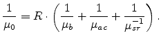
In this work, the surface mobility is thus modeled semi-empirically. A
formalism similar to that proposed by Darwish [Darwish97] is used.
Here the terms  ,
,  and
and  denote the bulk, acoustic
phonon, and surface roughness limited mobilities, respectively. The bulk
mobility is obtained by projecting the mobility tensor (4.45)
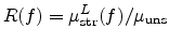
along the direction of the driving force vector. In the high effective field
regime, the inversion layer mobility is affected by surface acoustic phonons
and the mobility can be expressed as [Darwish97]
denote the bulk, acoustic
phonon, and surface roughness limited mobilities, respectively. The bulk
mobility is obtained by projecting the mobility tensor (4.45)
along the direction of the driving force vector. In the high effective field
regime, the inversion layer mobility is affected by surface acoustic phonons
and the mobility can be expressed as [Darwish97]
The formulation in (4.99) is based on the considerations of the
classical and quantum mechanical thickness of the inversion layer, as suggested
in [Schwarz83].  denotes the electric field component
perpendicular to the current direction.
denotes the electric field component
perpendicular to the current direction.
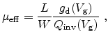
For very high effective fields, the mobility is limited by surface roughness
scattering and has been modeled as
The exponent  is a function of the local inversion charge. The increase
of the exponent with increasing inversion charge has been attributed to an
increase of inter-subband scattering at higher effective
fields [Mori79]. In (4.99) and (4.101), a doping dependence
is necessary in order to achieve an agreement between the measured and
calculated
is a function of the local inversion charge. The increase
of the exponent with increasing inversion charge has been attributed to an
increase of inter-subband scattering at higher effective
fields [Mori79]. In (4.99) and (4.101), a doping dependence
is necessary in order to achieve an agreement between the measured and
calculated
 .
.
The parameter  in (4.98) is a function of the enhancement factor
 and is given by
 |
(4.102) |
Here
 denotes the pure lattice mobility (excluding the
doping dependence) of strained Si and can be obtained by projecting the
mobility (4.45) along the direction of the driving force vector. The
experimental data in Fig. 4.7 reveal that the mobility enhancement is
higher for lower effective fields and vice-versa. To capture this effect into
the model, the enhancement factor has been modeled as
denotes the pure lattice mobility (excluding the
doping dependence) of strained Si and can be obtained by projecting the
mobility (4.45) along the direction of the driving force vector. The
experimental data in Fig. 4.7 reveal that the mobility enhancement is
higher for lower effective fields and vice-versa. To capture this effect into
the model, the enhancement factor has been modeled as
 |
(4.103) |
Next: 4.6 High-Field Mobility
Up: 4. Mobility Modeling
Previous: 4.4 Bulk Mobility of
S. Dhar: Analytical Mobility Modeling for Strained Silicon-Based Devices
![\includegraphics[width=3.0in,angle=0]{figures/sid_subbandUns.eps}](img629.png)
![\includegraphics[width=3.0in,angle=0]{figures/sid_subbandStr.eps}](img630.png)
![\includegraphics[width=3.0in]{figures/rot_EEeff1015-2.ps}](img656.png)
![$\displaystyle \mu_\ensuremath{{\mathrm{sr}}} = \left[D_1 + D_2 \cdot \left(\fra...
...\right] \left(\frac{S_\ensuremath{{\mathrm{ref}}}} {{E_\perp}}\right)^{\gamma},$](img663.png)
![\includegraphics[width=3.0in,angle=0]{figures/sid_SchematicEffmob2.eps}](img649.png)
![$\displaystyle \hspace*{-0cm} \mu_\ensuremath{{\mathrm{ac}}} = B\left(\frac{E_\e...
...t)^2\right] \left(\frac{E_\ensuremath{{\mathrm{ref}}}} {{E_\perp}}\right)^{1/3}$](img661.png)