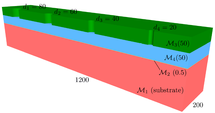
To demonstrate the multi-LS approach, an isotropic etching process is applied to the test structure given in Figure 4.10. The lateral extensions of this geometry are
![]() (in terms of grid spacings). The structure consists of three layers on top of a substrate. The layer thicknesses are, from top down,
(in terms of grid spacings). The structure consists of three layers on top of a substrate. The layer thicknesses are, from top down, ![]() ,
, ![]() , and
, and ![]() . The top layer is a mask with four circular holes with diameters
. The top layer is a mask with four circular holes with diameters ![]() ,
, ![]() ,
, ![]() , and
, and ![]() , respectively.
, respectively.
|
The way in which the different material regions are labeled defines the LS representation according to (4.19). Since underetching of the mask is expected, the mask is assigned to
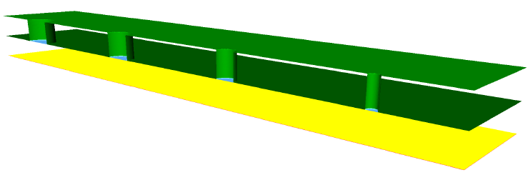
![]() . The complete numbering can be seen in Figure 4.10. The corresponding LS representation of the initial structure is depicted in Figure 4.11. Four LS functions are used to describe the four different material regions.
. The complete numbering can be seen in Figure 4.10. The corresponding LS representation of the initial structure is depicted in Figure 4.11. Four LS functions are used to describe the four different material regions.
|
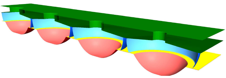
The multi-layer structure is exposed to an etch process. The etch rate is assumed to be ![]() grid spacings per time unit for the mask (
grid spacings per time unit for the mask (
![]() ) and
) and ![]() for the very thin layer (
for the very thin layer (
![]() ). For the other two material regions the etch rate is set to
). For the other two material regions the etch rate is set to ![]() . The profile after 120 time units is shown in Figure 4.12. Although the very thin layer has a thickness smaller than a grid spacing, its small etch rate is accurately incorporated during time evolution.
. The profile after 120 time units is shown in Figure 4.12. Although the very thin layer has a thickness smaller than a grid spacing, its small etch rate is accurately incorporated during time evolution.
|
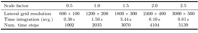
In order to prove the linear scaling of the entire time evolution algorithm, this etch process is applied to the same geometry, only scaled by various factors. The process times are scaled accordingly. Table 4.1 lists the average computation times for a single time step for scale factors 0.5, 1.0, 1.5, 2.0, and 2.5. The calculation time scales well with the surface size which itself scales quadratically with the scale factor. The total number of required time steps is also given. The numbers are obtained using
![]() . The simulation was carried out on an AMD Opteron 8222 SE processor with a CPU clock speed of
. The simulation was carried out on an AMD Opteron 8222 SE processor with a CPU clock speed of
![]() .
.