5.1 Defects in Amorphous Silicon Dioxide
This section deals with the basic properties of defects, especially the position of their
corresponding trap levels. Previous theoretical investigations were focused on defects
in crystalline  [112, 113] as a substitute for amorphous materials. At this
point it is emphasized that one has to consider the amorphous nature of
[112, 113] as a substitute for amorphous materials. At this
point it is emphasized that one has to consider the amorphous nature of
 since it strongly affects the defect properties: For instance, oxygen
molecules
since it strongly affects the defect properties: For instance, oxygen
molecules  in
in  have only discrete values for the barriers to migrate
from one void to the next one. By contrast in
have only discrete values for the barriers to migrate
from one void to the next one. By contrast in  , they encounter a
distribution of barriers whose average eventually determines the effective
activation energy for diffusion [167, 168]. Another example is the stability of the
, they encounter a
distribution of barriers whose average eventually determines the effective
activation energy for diffusion [167, 168]. Another example is the stability of the
 center, which can transform to an oxygen vacancy by overcoming a
thermal barrier. The height of this barrier and thus the stability of the
center, which can transform to an oxygen vacancy by overcoming a
thermal barrier. The height of this barrier and thus the stability of the  center have been found to strongly depend on the the local surrounding
silica network [19, 20]. These two examples suggest that small variations in
the bond lengths and angles of the surrounding structure could result in a
wide distribution of trap levels [162, 161] and thereby impact the trapping
dynamics. Unfortunately most of the defect properties are difficult to determine
experimentally so that theoretical methods, such as DFT, were chosen for the
determination of defect levels. The empirical potential molecular dynamics was
employed for the production of
center have been found to strongly depend on the the local surrounding
silica network [19, 20]. These two examples suggest that small variations in
the bond lengths and angles of the surrounding structure could result in a
wide distribution of trap levels [162, 161] and thereby impact the trapping
dynamics. Unfortunately most of the defect properties are difficult to determine
experimentally so that theoretical methods, such as DFT, were chosen for the
determination of defect levels. The empirical potential molecular dynamics was
employed for the production of  . The details of this procedure are
described in Section 3.4.2. Pair-correlation functions, angle distributions,
and the ring distribution have been evaluated in order to ensure that the
obtained samples mimic real
. The details of this procedure are
described in Section 3.4.2. Pair-correlation functions, angle distributions,
and the ring distribution have been evaluated in order to ensure that the
obtained samples mimic real  . The generated structures were used for
DFT calculations, whose parameters are summarized in Section 3.3.3. The
defect structures have been obtained by adding, shifting, or removing the
silicon, the oxygen, or the hydrogen atoms. The switching trap levels for the
created defects have been evaluated using the formulas (3.33)
. The generated structures were used for
DFT calculations, whose parameters are summarized in Section 3.3.3. The
defect structures have been obtained by adding, shifting, or removing the
silicon, the oxygen, or the hydrogen atoms. The switching trap levels for the
created defects have been evaluated using the formulas (3.33) (3.36). The
calculated trap levels have been aligned to the silicon bandgap using the
procedure proposed in [113]. The obtained valence band offset of
(3.36). The
calculated trap levels have been aligned to the silicon bandgap using the
procedure proposed in [113]. The obtained valence band offset of  for
the
for
the  interface has been found to be in good agreement with the
values extracted from [80, 169, 170]. In the following, a study of several
prominent defects in
interface has been found to be in good agreement with the
values extracted from [80, 169, 170]. In the following, a study of several
prominent defects in  will be presented. They will be discussed based
on their configuration in their various charge states in order to check the
correctness of the produced defect structures. Furthermore, their expected
trapping behavior will be inferred from the switching levels gained from DFT
simulations.
will be presented. They will be discussed based
on their configuration in their various charge states in order to check the
correctness of the produced defect structures. Furthermore, their expected
trapping behavior will be inferred from the switching levels gained from DFT
simulations.
5.1.1 Oxygen Vacancy
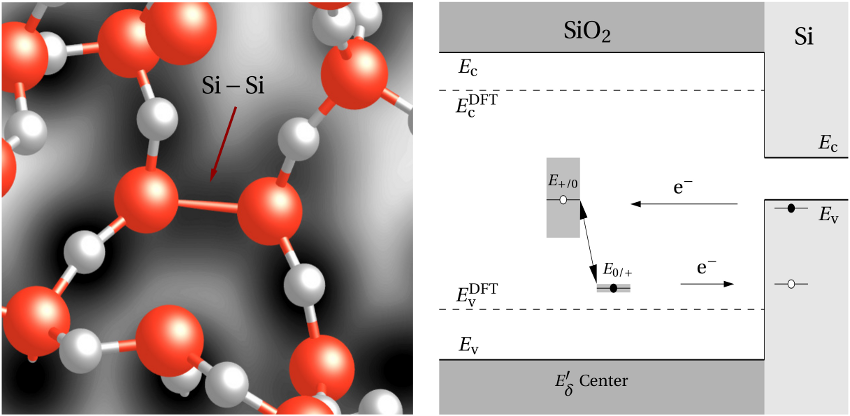
In stoichiometric  , two silicon atoms are always connected by one bridging
oxygen atom. When this atom is removed, the two neighboring silicon atoms
establish a common bond, the heart of the oxygen vacancy (see Fig. 5.1). In
, two silicon atoms are always connected by one bridging
oxygen atom. When this atom is removed, the two neighboring silicon atoms
establish a common bond, the heart of the oxygen vacancy (see Fig. 5.1). In
 , the length of this bond is approximately
  [19, 149], which compares
well with the
[19, 149], which compares
well with the  -
- distance of
  in crystalline bulk silicon [171]. In the DFT
simulations of this thesis, the defects are embedded in an amorphous
in crystalline bulk silicon [171]. In the DFT
simulations of this thesis, the defects are embedded in an amorphous  host
material so that this characteristic length is distributed. Our set of structures
covers
host
material so that this characteristic length is distributed. Our set of structures
covers  -
- bond lengths between
  and
and  . These values are in
reasonable agreement with the range (
. These values are in
reasonable agreement with the range ( ) obtained in the study of
Mukhopadhyay et al. [172]. Nicklaw [162] extended his defect calculations to
highly strained oxygen vacancies whose bond lengths reach values up to
) obtained in the study of
Mukhopadhyay et al. [172]. Nicklaw [162] extended his defect calculations to
highly strained oxygen vacancies whose bond lengths reach values up to  . This
kind of defects is associated with large formation energies [173], thus exists
in small concentrations, and has a negligible contribution to the trapping
kinetics of NBTI. The
. This
kind of defects is associated with large formation energies [173], thus exists
in small concentrations, and has a negligible contribution to the trapping
kinetics of NBTI. The  -
- bond is associated with the
  level,
which is sharply peaked and situated far below the silicon valence band
edge (cf. Fig. 5.1 and Table 5.1). For comparison, the corresponding defect
calculations in
level,
which is sharply peaked and situated far below the silicon valence band
edge (cf. Fig. 5.1 and Table 5.1). For comparison, the corresponding defect
calculations in  [149] predict
  at approximately the same
position.
at approximately the same
position.
In the context of EPR measurements, the positively charged counterpart of the
oxygen vacancy is referred to as the  center. The missing negative charge within
its bond causes a repulsion between the two electropositive silicon atoms and
results in a stretching but not in a breakage of the
center. The missing negative charge within
its bond causes a repulsion between the two electropositive silicon atoms and
results in a stretching but not in a breakage of the  bond. In the
 reference, the
  -
- bond of
  center was found to extend from
 to
to  [149, 19], which is large in comparison to the bond length
of a neutral oxygen vacancy. In the DFT simulations of this thesis, this
kind of weak bonds experiences large tensile and compressive forces due the
amorphous
[149, 19], which is large in comparison to the bond length
of a neutral oxygen vacancy. In the DFT simulations of this thesis, this
kind of weak bonds experiences large tensile and compressive forces due the
amorphous  host material. The corresponding bond lengths are found to be
distributed within a range of
host material. The corresponding bond lengths are found to be
distributed within a range of  , consistent with the values used in [19]
and [20]. This
, consistent with the values used in [19]
and [20]. This  -
- bond is associated with a defect level close to the
silicon valence band edge. Due to the amorphous nature of
bond is associated with a defect level close to the
silicon valence band edge. Due to the amorphous nature of  , the defect
levels
, the defect
levels  are spread widely over an energy range from
  to
to
 (cf. Fig. 5.1). By contrast in the case of the neutral oxygen vacancy
the impact of the surrounding network can be neglected due to the strong
(cf. Fig. 5.1). By contrast in the case of the neutral oxygen vacancy
the impact of the surrounding network can be neglected due to the strong
 bond so that the distribution of
  levels is narrow as shown in
Fig. 5.1.
levels is narrow as shown in
Fig. 5.1.
Regarding the tunneling dynamics, one has to differentiate between two cases:
If the defect level  is located below the silicon valence band edge,
electrons from the substrate valence band can be captured by the defect via
elastic tunneling. For the reverse process, the defect level is already shifted
downwards, where the electron in the defect is unlikely to find a high energetic
hole in the substrate. From this argumentation it is expected that oxygen
vacancy remains neutral if it is discharged once. In case the
is located below the silicon valence band edge,
electrons from the substrate valence band can be captured by the defect via
elastic tunneling. For the reverse process, the defect level is already shifted
downwards, where the electron in the defect is unlikely to find a high energetic
hole in the substrate. From this argumentation it is expected that oxygen
vacancy remains neutral if it is discharged once. In case the  level is
located above the silicon valence band edge, electron capture into the defect is
inhibited, which suggests that this defect acts as a ‘fixed positive charge’.
However, keep in mind that these charges may be neutralized via interface states
instead.
level is
located above the silicon valence band edge, electron capture into the defect is
inhibited, which suggests that this defect acts as a ‘fixed positive charge’.
However, keep in mind that these charges may be neutralized via interface states
instead.
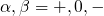
5.1.2  Center and Variants
The existence of the  center as an additional metastable configuration of the
oxygen vacancy has been confirmed by a wide range of theoretical [20, 19] as well as
experimental [15, 16] studies. Starting from the
center as an additional metastable configuration of the
oxygen vacancy has been confirmed by a wide range of theoretical [20, 19] as well as
experimental [15, 16] studies. Starting from the  center, one side of the defect
undergoes a transformation called ‘puckered’. During this, the dimer bond is
disrupted and the ‘puckered’ silicon atom moves through the plane defined by its
three oxygen neighbors where this new configuration is stabilized via a back bond to
a nearby oxygen atom. In the DFT simulations of this thesis, the back bond has
typically a length of
center, one side of the defect
undergoes a transformation called ‘puckered’. During this, the dimer bond is
disrupted and the ‘puckered’ silicon atom moves through the plane defined by its
three oxygen neighbors where this new configuration is stabilized via a back bond to
a nearby oxygen atom. In the DFT simulations of this thesis, the back bond has
typically a length of  , which is large compared to the
  -
- bond in
bulk
bond in
bulk  (
( ) [174, 155, 153, 154]. This indicates a weak bonding
of the ‘puckering’ silicon atom to the back oxygen. On the other side of
this defect, an unsaturated silicon dangling bond is left behind, which can
carry up to two electrons and gives an EPR signal [17]. Only if the
) [174, 155, 153, 154]. This indicates a weak bonding
of the ‘puckering’ silicon atom to the back oxygen. On the other side of
this defect, an unsaturated silicon dangling bond is left behind, which can
carry up to two electrons and gives an EPR signal [17]. Only if the  center is neutralized, this defect is prone to a collapse into its oxygen vacancy
configuration [20] again. The configuration of the
center is neutralized, this defect is prone to a collapse into its oxygen vacancy
configuration [20] again. The configuration of the  center is depicted in
Fig. 5.2.
center is depicted in
Fig. 5.2.
In contrast to the oxygen vacancy, the defect levels  and
and  of the
  center have only a small spread of about
  since the silicon dangling bond
along with the three other
since the silicon dangling bond
along with the three other  bonds almost preserve their tetrahedral symmetry
during structural relaxation. The puckered side of the defect complex does not
interact with the dangling bond and consequently does not impact its defect levels.
The levels for tunneling into (
bonds almost preserve their tetrahedral symmetry
during structural relaxation. The puckered side of the defect complex does not
interact with the dangling bond and consequently does not impact its defect levels.
The levels for tunneling into ( ) or out of (
 ) the traps lie close to the
silicon band edges (see Fig. 5.3). Therefore, only a small thermal excitation of the
substrate charge carriers is required for a tunneling process. In this case, the band
bending controls the concentrations of electrons in the silicon conduction band or
holes in the silicon valence band, respectively, and consequently governs the
tunneling rates. This means that the
) the traps lie close to the
silicon band edges (see Fig. 5.3). Therefore, only a small thermal excitation of the
substrate charge carriers is required for a tunneling process. In this case, the band
bending controls the concentrations of electrons in the silicon conduction band or
holes in the silicon valence band, respectively, and consequently governs the
tunneling rates. This means that the  centers can be repeatedly charged and
discharged by electrons by switching the MOSFET between strong inversion and
accumulation. The
centers can be repeatedly charged and
discharged by electrons by switching the MOSFET between strong inversion and
accumulation. The  configuration was already proposed by Lelis [15, 16] in the
context of the temperature-dependent annealing behavior of oxide traps. The
temperature dependence in his model was explained by a transition from a
spin-triplet [15] to its corresponding spin-singlet state. The latter denotes the ground
state of two electrons, which sit in the dangling bond of an
configuration was already proposed by Lelis [15, 16] in the
context of the temperature-dependent annealing behavior of oxide traps. The
temperature dependence in his model was explained by a transition from a
spin-triplet [15] to its corresponding spin-singlet state. The latter denotes the ground
state of two electrons, which sit in the dangling bond of an  center and
have their spins aligned anti-parallel. The spin-triplet state is the excited
counterpart, which is characterized by a parallel alignment of the electron spins and
decays immediately to the spin-singlet ground state after it is occupied.
According to the argumentation of Lelis, the concentration of thermally
excited electrons is increased at elevated temperatures. This gives rise to an
enhanced tunneling probability and thus an accelerated annealing of positively
charged
center and
have their spins aligned anti-parallel. The spin-triplet state is the excited
counterpart, which is characterized by a parallel alignment of the electron spins and
decays immediately to the spin-singlet ground state after it is occupied.
According to the argumentation of Lelis, the concentration of thermally
excited electrons is increased at elevated temperatures. This gives rise to an
enhanced tunneling probability and thus an accelerated annealing of positively
charged  centers. Interestingly, the energy level of the excited spin-triplet
state [15] coincides with the electron capture level
centers. Interestingly, the energy level of the excited spin-triplet
state [15] coincides with the electron capture level  obtained by the DFT
simulations of this thesis. Thus, the level shift can explain the same trapping
dynamics as in Lelis when replacing the spin-triplet state with the
obtained by the DFT
simulations of this thesis. Thus, the level shift can explain the same trapping
dynamics as in Lelis when replacing the spin-triplet state with the  level.
In this way, the defect levels responsible for the annealing behavior in the
Lelis model has been theoretically confirmed but with the interpretation
based on the level shift. As highlighted in [20], most of the
level.
In this way, the defect levels responsible for the annealing behavior in the
Lelis model has been theoretically confirmed but with the interpretation
based on the level shift. As highlighted in [20], most of the  centers
immediately collapses into their oxygen vacancy configuration after neutralization.
Then they feature defect levels, located down far below the silicon valence
band edge. Therefore, once these defects are neutralized, they cannot be
recharged again and will be permanently annealed out. However, this does
not rule out the
centers
immediately collapses into their oxygen vacancy configuration after neutralization.
Then they feature defect levels, located down far below the silicon valence
band edge. Therefore, once these defects are neutralized, they cannot be
recharged again and will be permanently annealed out. However, this does
not rule out the  center as a cycling charge. A considerable fraction of
the neutralized
center as a cycling charge. A considerable fraction of
the neutralized  centers [20] have a large barrier for the relaxation to
the oxygen vacancy configuration and thus may remain in the puckered
configuration for time scales relevant for NBTI. In this configuration, they
are capable of repeatedly exchanging electrons or holes with the
centers [20] have a large barrier for the relaxation to
the oxygen vacancy configuration and thus may remain in the puckered
configuration for time scales relevant for NBTI. In this configuration, they
are capable of repeatedly exchanging electrons or holes with the  interface.
Another variant of the  center is the
  center (shown in Fig. 5.4), which has
been extensively studied by Conley and Lenahan [40]. Its structure can be visualized
by replacing one of the nearby oxygen atoms with an hydrogen atom. The DFT
simulations in this thesis have revealed that the neighboring hydrogen atom does not
affect the position of the defect levels originating from the dangling bond.
As a result, this defect features the same distribution of trap levels and
therefore can be repeatedly charged and discharged similarly to the simple
center (shown in Fig. 5.4), which has
been extensively studied by Conley and Lenahan [40]. Its structure can be visualized
by replacing one of the nearby oxygen atoms with an hydrogen atom. The DFT
simulations in this thesis have revealed that the neighboring hydrogen atom does not
affect the position of the defect levels originating from the dangling bond.
As a result, this defect features the same distribution of trap levels and
therefore can be repeatedly charged and discharged similarly to the simple  center.
5.1.3 Hydrogen Atom
In the context of reliability issues, the hydrogen atom [175, 176] is of special interest
since it is available in appreciable amounts. Indeed it has been speculated in many
investigations [177, 149] that hydrogen seriously affects the reliability of MOSFETs.
Its configuration strongly differs with its charge state: The DFT simulations of this
thesis predict the neutral atom  in the middle of a void where it does not form a
bond with any
in the middle of a void where it does not form a
bond with any  network atom, consistent with DFT investigations in
 [175, 176]. The positively charged atom
  weakly binds to one of the
electronegative oxygen network atoms as shown in Fig. 5.5. The corresponding
weakly binds to one of the
electronegative oxygen network atoms as shown in Fig. 5.5. The corresponding
 -
- bond length is found to be approximately
  , which compares
perfectly well with the values for
, which compares
perfectly well with the values for  (
( ) in [164] and
  (
( ) in [149, 176]. The negatively charged atom
  attaches to an
electropositive silicon atom with a bond distance of about
attaches to an
electropositive silicon atom with a bond distance of about  , in agreement
with [164, 176, 149].
, in agreement
with [164, 176, 149].
The energy levels of the hydrogen atom are visualized in Fig. 5.6 and listed in
Table 5.1. The trap levels  ,
,  , and
, and  are located far away from the
silicon band edges and consequently require highly excited substrate charge
carriers for a tunneling transition. By contrast,
are located far away from the
silicon band edges and consequently require highly excited substrate charge
carriers for a tunneling transition. By contrast,  is centered around the
silicon conduction band edge, resulting in a high tunneling probability. This
suggests that the defect is preferredly found in its negative charge state
at a weak oxide field. At a first glance, this result seems to contradict the
findings of other groups [176, 175, 149]. According to them, the proton has
been predicted to be the most stable charge state of the hydrogen atom.
However, the calculations are based on a thermodynamic transition level, which
only applies to thermally-activated processes, such as NMP transitions for
instance.
is centered around the
silicon conduction band edge, resulting in a high tunneling probability. This
suggests that the defect is preferredly found in its negative charge state
at a weak oxide field. At a first glance, this result seems to contradict the
findings of other groups [176, 175, 149]. According to them, the proton has
been predicted to be the most stable charge state of the hydrogen atom.
However, the calculations are based on a thermodynamic transition level, which
only applies to thermally-activated processes, such as NMP transitions for
instance.
5.1.4 Hydrogen Bridge
Hydrogen is frequently suspected to undergo reactions with oxide defects [178, 179].
Therefore, the present investigations include a hydrogenated variant of the  center, also referred to as the hydrogen bridge (see Fig. 5.7). This defect can
be constructed by placing a hydrogen atom inbetween the silicon dimer of
an oxygen vacancy. In the positive charge state, the hydrogen atom forms
a three-center bond involving the two silicon atoms from the dimer and
the hydrogen atom in the central position. Its relaxed structure exhibits an
asymmetry in the
center, also referred to as the hydrogen bridge (see Fig. 5.7). This defect can
be constructed by placing a hydrogen atom inbetween the silicon dimer of
an oxygen vacancy. In the positive charge state, the hydrogen atom forms
a three-center bond involving the two silicon atoms from the dimer and
the hydrogen atom in the central position. Its relaxed structure exhibits an
asymmetry in the  -
- distances with values of
  and
and  .
This is in qualitative agreement with the corresponding defect structure
generated in
.
This is in qualitative agreement with the corresponding defect structure
generated in  [149], however, there are small deviations in the
 -
- distances attributed to variations in the atomic structure of the
 host structure. Note that although the aforementioned three-center
bond is generally considered unusual in chemistry, the same
host structure. Note that although the aforementioned three-center
bond is generally considered unusual in chemistry, the same  -
- -
- bond chain has also been observed for
  in
in  [180]. In the neutral
charge state, the three-center bond is disrupted on the side with the long
[180]. In the neutral
charge state, the three-center bond is disrupted on the side with the long
 distance. The breakage is accompanied by a large structural relaxation
which detaches the
distance. The breakage is accompanied by a large structural relaxation
which detaches the  -
- complex from the remaining dangling bond.
The
complex from the remaining dangling bond.
The  bond length reduces to its typical value of
  [181] for the
unperturbed
[181] for the
unperturbed  -
- bond while the other silicon atom is separated from
the hydrogen atom by about
bond while the other silicon atom is separated from
the hydrogen atom by about  and carries one electron in its
dangling bond orbital. By contrast, Blöchl et al. [149] found that even in the
neutral charge state the hydrogen atom interacts with both silicon atoms.
This discrepancy may originate from the rigid network of the surrounding
and carries one electron in its
dangling bond orbital. By contrast, Blöchl et al. [149] found that even in the
neutral charge state the hydrogen atom interacts with both silicon atoms.
This discrepancy may originate from the rigid network of the surrounding
 , which keeps both silicon atoms together and thus prevents the
 -
- -
- chain from bond breakage in the neutral charge state. In the
negative charge state, the added electron sits on the dangling bond and causes
a further repulsion between the dangling bond and the
chain from bond breakage in the neutral charge state. In the
negative charge state, the added electron sits on the dangling bond and causes
a further repulsion between the dangling bond and the  -
- complex
(
complex
( ).
).
As shown in Fig. 5.8 and Table 5.1, all defect levels are located within a reasonable
distance from silicon band edges on the energy scale. This suggests that
none of the considered transitions can be ruled out based on the positon of
its corresponding trap level. Thus the trapping dynamics are eventually
governed by the band bending in the substrate and the operation state of the
MOSFET.
 -
- bond, established after the
removal of an oxygen atom, is indicated by a high charge density (dark area)
between the neighboring silicon atoms.
bond, established after the
removal of an oxygen atom, is indicated by a high charge density (dark area)
between the neighboring silicon atoms.  centers (positively charged) in
  .
.
 (dashed line) denotes the conduction/valence band edge, extracted from
the DFT simulations. The
(dashed line) denotes the conduction/valence band edge, extracted from
the DFT simulations. The  levels are related to the capture of electrons
while the
levels are related to the capture of electrons
while the  levels apply to electron emission. The double-sided arrow
represents the shift of defect levels and the spreads of energy levels are visualized
by the grey boxes.
levels apply to electron emission. The double-sided arrow
represents the shift of defect levels and the spreads of energy levels are visualized
by the grey boxes.


 ,
,  , etc.) referenced to the midgap of
the substrate silicon. The first sign of
, etc.) referenced to the midgap of
the substrate silicon. The first sign of  (
( ) indicates the
equilibrium configuration of the defect in the corresponding charge state and
the second sign gives the charge state of the defect for a given configuration.
) indicates the
equilibrium configuration of the defect in the corresponding charge state and
the second sign gives the charge state of the defect for a given configuration.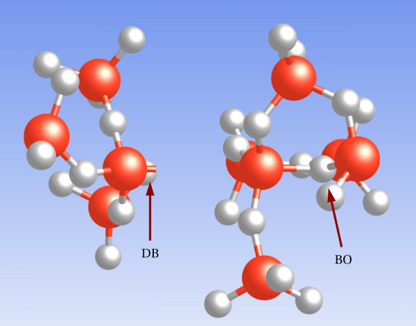
 center. The silicon atom on the left of
the oxygen vacancy can carry up to two electrons in the dangling bond (DB),
which is indicated by the stick only connected to the silicon atom. The positively
charged silicon atom on the right-hand side is bonded to the back oxygen (BO).
The above atomic arrangement is also referred to as the puckered configuration.
center. The silicon atom on the left of
the oxygen vacancy can carry up to two electrons in the dangling bond (DB),
which is indicated by the stick only connected to the silicon atom. The positively
charged silicon atom on the right-hand side is bonded to the back oxygen (BO).
The above atomic arrangement is also referred to as the puckered configuration.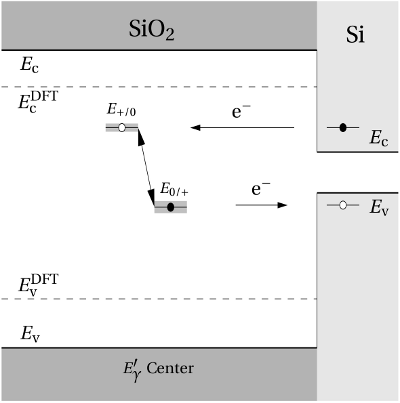
 centers in
  .
The energy levels for the capture of electrons (
.
The energy levels for the capture of electrons ( ) as well as the energy
levels for the emission of electrons (
) as well as the energy
levels for the emission of electrons ( ) are found to lie close to the silicon
conduction or valence band, respectively.
) are found to lie close to the silicon
conduction or valence band, respectively.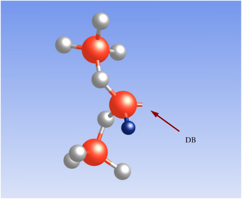
 center. The blue sphere represents an
hydrogen atom. One of the neighboring O atoms is replaced by an hydrogen
atom which shows a tendency to bond to a silica network atom.
center. The blue sphere represents an
hydrogen atom. One of the neighboring O atoms is replaced by an hydrogen
atom which shows a tendency to bond to a silica network atom.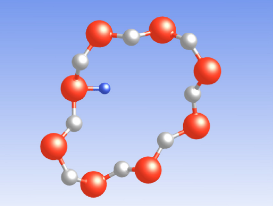
 attaches to the bridging oxygen atom,
  is situated in
the middle of a void, and
is situated in
the middle of a void, and  forms a weak bond to a silicon network atom.
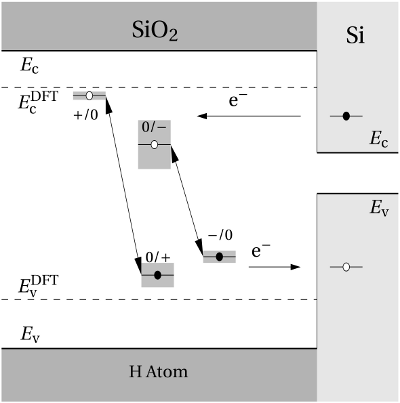
 . The energy
levels for charging and discharging are far away from the respective silicon band
edges. Except of
. The energy
levels for charging and discharging are far away from the respective silicon band
edges. Except of  , all defect levels are largely separated from the band
edges and thus unlikely to find a high energetic charge carrier for a tunneling
transition.
, all defect levels are largely separated from the band
edges and thus unlikely to find a high energetic charge carrier for a tunneling
transition.
 -
- -
- bond chain.
After neutralization this chain is disrupted yielding a dangling bond on the left
hand side of this complex and a saturated dangling bond on the right-hand side.
In the case of a negatively charged hydrogen bridge, the
bond chain.
After neutralization this chain is disrupted yielding a dangling bond on the left
hand side of this complex and a saturated dangling bond on the right-hand side.
In the case of a negatively charged hydrogen bridge, the  -
- bond is bent
away from the dangling bond.
bond is bent
away from the dangling bond.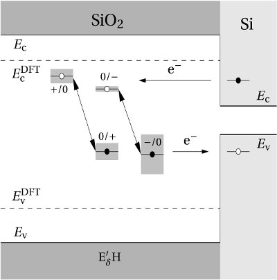
 . The hole
(
. The hole
( and
and  ) capture levels lie slightly closer to the substrate bandgap
compared to the electron (
) capture levels lie slightly closer to the substrate bandgap
compared to the electron ( and
and  ) levels. This indicates that the
hydrogen bridge favors the positive charge state. In the end, the operation state
of the MOSFET will eventually determine the charge state of the defect.
) levels. This indicates that the
hydrogen bridge favors the positive charge state. In the end, the operation state
of the MOSFET will eventually determine the charge state of the defect.