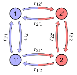
Figure 7.2: Left: A schematic of the configuration coordinate diagram for a
bistable defect. The solid red and the blue dashed lines represent the adiabatic
potentials for a defect in its positive and neutral charge state, respectively. The
energy minima correspond to the stable or metastable defect configurations,
labeled by  with
with  . The present configuration coordinate diagram
describes the exchange of holes with the valence band and thus is associated with
a hole capture or emission process. The stick-and-ball models display a defect in
its various stable and metastable configurations. A possible candidate for such a
bistable defect might be the well-known
. The present configuration coordinate diagram
describes the exchange of holes with the valence band and thus is associated with
a hole capture or emission process. The stick-and-ball models display a defect in
its various stable and metastable configurations. A possible candidate for such a
bistable defect might be the well-known  center, which is frequently invoked
in the context of noise in MOSFETs. Right: Definitions of the used energies and
barriers in the eNMP model. Recall that two adiabatic potentials must be shown
for one transition. It is assumed that an alternative transition pathway with an
additional crossing point exists in the multi-dimensional atomic configuration
space. In order to show both intersections (related to
center, which is frequently invoked
in the context of noise in MOSFETs. Right: Definitions of the used energies and
barriers in the eNMP model. Recall that two adiabatic potentials must be shown
for one transition. It is assumed that an alternative transition pathway with an
additional crossing point exists in the multi-dimensional atomic configuration
space. In order to show both intersections (related to  and
and  ) in
one configuration coordinate diagram, the ‘neutral’ potential must be plotted
twice. Obviously,
) in
one configuration coordinate diagram, the ‘neutral’ potential must be plotted
twice. Obviously,  and
and  hold.
hold.
with . The present configuration coordinate diagram
describes the exchange of holes with the valence band and thus is associated with
a hole capture or emission process. The stick-and-ball models display a defect in
its various stable and metastable configurations. A possible candidate for such a
bistable defect might be the well-known center, which is frequently invoked
in the context of noise in MOSFETs. Right: Definitions of the used energies and
barriers in the eNMP model. Recall that two adiabatic potentials must be shown
for one transition. It is assumed that an alternative transition pathway with an
additional crossing point exists in the multi-dimensional atomic configuration
space. In order to show both intersections (related to and ) in
one configuration coordinate diagram, the ‘neutral’ potential must be plotted
twice. Obviously, and hold. and
and  denote the positive and neutral charge
state of the defect, respectively, and the metastable states are marked
by additional primes. In the configuration coordinate diagram, there
exist two crossing points, where each of them is related to one of the two
charge transfer reactions
denote the positive and neutral charge
state of the defect, respectively, and the metastable states are marked
by additional primes. In the configuration coordinate diagram, there
exist two crossing points, where each of them is related to one of the two
charge transfer reactions  and
and  . Their corresponding NMP
barriers
. Their corresponding NMP
barriers and
and  are derived by evaluating equation (
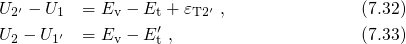
 are expected to be within the same order of magnitude for all
charge transfer reactions and are thus set equal. The field dependence of the charge
transfer reactions
are expected to be within the same order of magnitude for all
charge transfer reactions and are thus set equal. The field dependence of the charge
transfer reactions  and
and  is governed by the relative position of the
‘neutral’ and the ‘positive’ adiabatic potential. When a negative bias is applied to the
gate of a pMOSFET (see Fig. 7.2), the ‘neutral’ potential is raised. As a result, the
barriers
is governed by the relative position of the
‘neutral’ and the ‘positive’ adiabatic potential. When a negative bias is applied to the
gate of a pMOSFET (see Fig. 7.2), the ‘neutral’ potential is raised. As a result, the
barriers  and
and  are reduced, which facilitates the charge transfer reactions
 and
and  , respectively. Conversely, the transitions
  and
and  are
slowed down since the corresponding barrier heights
are
slowed down since the corresponding barrier heights  and
and  have become
larger. The transitions
have become
larger. The transitions  and
and  are thermally activated and do not vary
with the applied gate bias. According to transition state theory, they can be
expressed as
are thermally activated and do not vary
with the applied gate bias. According to transition state theory, they can be
expressed as 
 are defined as in Fig. 7.2 and
  stands for the attempt
frequency, which is typically of the order
stands for the attempt
frequency, which is typically of the order  . Using
  and
and 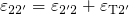 , the rates
  and
and  can be rewritten as