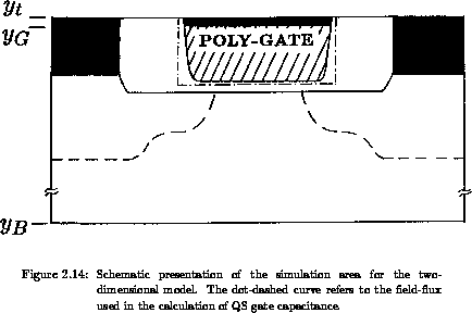
An obvious approach to include the non-equipotential gate in a device simulator like MINIMOS [415][160] is to solve numerically the discretized continuity equations with the Poisson equation in the polysilicon gate, simultaneously with the silicon bulk [163]. The simulation structure is displayed in Figure 2.14. An enlarged mesh, due to resolving the gate/oxide interface, and the space charge in the gate do not pose additional difficulties in solving the Poisson equation, which is a quite stable numerical problem. In contrast, solving the continuity equations in the gate area significantly increases the computational burden, since these equations consume the largest portion of the total calculation time. Therefore, this approach is interesting solely for transient conditions, where the currents become nonzero in the gate. For the steady-state a much more efficient approach may be proposed as is introduced later, because the currents as well as the net generation-recombination vanish in the gate.
However, for a moment let us consider transient effects that can occur in
nondegenerate gates. In MOSFETs, source and drain are efficient
suppliers of minority carriers for the channel. Quasi-static conditions can be
maintained up to a high frequency ( MHz or more) in the channel, which depends
in the first place on the channel length
MHz or more) in the channel, which depends
in the first place on the channel length  . There is no external supply of
minorities in the gate. Thereby, transient effects occurring in MOS capacitors
due to finite minority carrier response may be expected to occur in
nondegenerate gates:
. There is no external supply of
minorities in the gate. Thereby, transient effects occurring in MOS capacitors
due to finite minority carrier response may be expected to occur in
nondegenerate gates:
 -type gate electrons tunnel from the valence
band close to the gate/oxide interface towards the conduction band
remote from the interface, while holes are left at the interface
contributing in the formation of the inversion layer. Due to high
doping in the gate, the depletion region is shallow even for large
band-bending. For example: if
-type gate electrons tunnel from the valence
band close to the gate/oxide interface towards the conduction band
remote from the interface, while holes are left at the interface
contributing in the formation of the inversion layer. Due to high
doping in the gate, the depletion region is shallow even for large
band-bending. For example: if  of only
  is achieved
by pulsing the gate into deep-depletion, the minimal tunneling
length becomes
is achieved
by pulsing the gate into deep-depletion, the minimal tunneling
length becomes  and the surface field
  for doping of
  . Assuming a doping of
 , it follows
  and
and  . Since the BBT rate can be very large, we
expect that this mechanism may clamp further increasing in
when forcing the gate into deep-depletion. To prove this claim,
however, selfconsistent transient simulation is necessary
(Section 3.2), including BBT
(Section 4.2) in the gate.
. Since the BBT rate can be very large, we
expect that this mechanism may clamp further increasing in
when forcing the gate into deep-depletion. To prove this claim,
however, selfconsistent transient simulation is necessary
(Section 3.2), including BBT
(Section 4.2) in the gate.
 -type
gate because of a lower barrier for electrons than for holes.
-type
gate because of a lower barrier for electrons than for holes.
 ) capacitance in an -type gate (-channel
devices) [269][226]. Moreover, for highly resistive gates a very
slow turn-off is measured in the drain current in [226], as well.
) capacitance in an -type gate (-channel
devices) [269][226]. Moreover, for highly resistive gates a very
slow turn-off is measured in the drain current in [226], as well.
Steady-state two-dimensional numerical model:
Henceforward we assume steady-state conditions. Due to quasi-equilibrium in the
gate, as already pointed out in Section 2.2, carrier
concentrations and may be calculated analytically as a function of
the local potential  , instead of solving the continuity equations,
particularly when the latter must be discretized accounting for FD
statistics [166][163]. For
, instead of solving the continuity equations,
particularly when the latter must be discretized accounting for FD
statistics [166][163]. For  and
and  the
relationships 2.10 and 2.11 are implemented in
a two-dimensional numerical model. Since solving the continuity equations is
restricted to bulk, this approach demands nearly the same computational effort
as the conventional MOSFET simulation with the equipotential gate. As boundary
conditions at the ohmic gate/polysilicon interface (gate-contact) the potential
the
relationships 2.10 and 2.11 are implemented in
a two-dimensional numerical model. Since solving the continuity equations is
restricted to bulk, this approach demands nearly the same computational effort
as the conventional MOSFET simulation with the equipotential gate. As boundary
conditions at the ohmic gate/polysilicon interface (gate-contact) the potential
 is given by 2.12, whereas neutrality is assumed for
the carrier concentrations, leading to equations 2.13
and 2.14. The approximations to the Fermi integral
is given by 2.12, whereas neutrality is assumed for
the carrier concentrations, leading to equations 2.13
and 2.14. The approximations to the Fermi integral
 and its inverse
  are clarified in
Appendix A. Note that in this approach we still need to increase
the mesh-size due to a finite thickness of the gate if we are particularly
interested in the gate-side or gate-corner effects, like fringing capacitances
and corner fields. For most analyses this is not necessary and the gate
depletion can be implemented in an even simpler and more efficient way than
this, as explained below.
are clarified in
Appendix A. Note that in this approach we still need to increase
the mesh-size due to a finite thickness of the gate if we are particularly
interested in the gate-side or gate-corner effects, like fringing capacitances
and corner fields. For most analyses this is not necessary and the gate
depletion can be implemented in an even simpler and more efficient way than
this, as explained below.
Quasi-two-dimensional approach:
Remember that denotes the difference between the potential at the
gate/oxide interface and the gate-contact potential (determined by
 ). In MOSFETs
  varies along the gate/oxide interface.
Note that
varies along the gate/oxide interface.
Note that  and
and  are the coordinates parallel and perpendicular to the
interface, respectively. It is obvious that the value of can range from
roughly
are the coordinates parallel and perpendicular to the
interface, respectively. It is obvious that the value of can range from
roughly  in strong accumulation to
  in strong inversion assuming
an -type gate. As a consequence the maximum difference between the potential
at the drain-side and the source-side of the gate is limited to about
in strong inversion assuming
an -type gate. As a consequence the maximum difference between the potential
at the drain-side and the source-side of the gate is limited to about  ,
whereas the corresponding difference in the channel is roughly
,
whereas the corresponding difference in the channel is roughly  .
Therefore, the gate may be considered to be an MOS device with a moderate
drain-source bias in the direction. In these devices the
gradual-channel-approximation (G.C.A.)
.
Therefore, the gate may be considered to be an MOS device with a moderate
drain-source bias in the direction. In these devices the
gradual-channel-approximation (G.C.A.)
 and the capacitance relation
  are reasonable
assumptions near the interface. To estimate the lateral field at the
interface in the gate
are reasonable
assumptions near the interface. To estimate the lateral field at the
interface in the gate  , remark that
relationships 2.4 and 2.6 are valid
in general (
, remark that
relationships 2.4 and 2.6 are valid
in general ( is the transversal component of the surface field). Applying
 on these formulas with benefit of
 , we derive
which is valid in general.  is the lateral
field at the interface in the bulk. If G.C.A. is valid in the bulk
is the lateral
field at the interface in the bulk. If G.C.A. is valid in the bulk
 is always positive and
 follows from 2.28.
Because of
follows from 2.28.
Because of  in the bulk and the
relation between
in the bulk and the
relation between  and given by 2.2,
 is valid (rigorously, always when
no interface charge is presented). The preceding analysis may be applied to the
complete channel if the MOSFET is biased in linear (triode) region. For MOSFET
is in saturation, the G.C.A. holds in the so-called source channel-part
([162][161] and references cited therein). Moreover, it is valid
in the corresponding part of the gate as well - just on the other side of the
oxide. The G.C.A. does not hold in the drain channel-part after the pinch-off
point and probably vis-à-vis in the gate too. However, this fact is
irrelevant, since the gate has lost its influence on the bulk in the
drain-channel part. Consequently, where
the gate controls the channel, the G.C.A. holds in the gate. We may conclude
that, unlike for the bulk, two-dimensional effects are of second order
importance in the gate, except at the corners.
is valid (rigorously, always when
no interface charge is presented). The preceding analysis may be applied to the
complete channel if the MOSFET is biased in linear (triode) region. For MOSFET
is in saturation, the G.C.A. holds in the so-called source channel-part
([162][161] and references cited therein). Moreover, it is valid
in the corresponding part of the gate as well - just on the other side of the
oxide. The G.C.A. does not hold in the drain channel-part after the pinch-off
point and probably vis-à-vis in the gate too. However, this fact is
irrelevant, since the gate has lost its influence on the bulk in the
drain-channel part. Consequently, where
the gate controls the channel, the G.C.A. holds in the gate. We may conclude
that, unlike for the bulk, two-dimensional effects are of second order
importance in the gate, except at the corners.
According to the preceding discussion one can assume the problem to be
one-dimensional in the gate area. The surface potential depends only
on the local perpendicular field in the polysilicon at the interface
and can be calculated by solving equation 2.16 for FD
statistics or A.14 for MB statistics. Furthermore, if one has no
interest in the gate-side effects, the actual gate thickness can be neglected.
The model reduces to the conventional planar MOSFET simulation, but with the
gate-contact potential variable along the coordinate:  .
In MINIMOS, this is implemented by updating the gate potential boundary
condition after each Poisson/continuity equation solution-step by calculating
for a given local
.
In MINIMOS, this is implemented by updating the gate potential boundary
condition after each Poisson/continuity equation solution-step by calculating
for a given local  and an interface charge
  ,
up to selfconsistency. This calculation is very fast compared to two-dimensional
solution of the Poisson equation in the gate. Moreover, the additional and
grid lines necessary to resolve the gate/oxide interface, as well as grid
adaptation are avoided. In this approach, the damping of the potential changes
applied to the gate may be employed to accelerate the convergence of the
simulation [160].
,
up to selfconsistency. This calculation is very fast compared to two-dimensional
solution of the Poisson equation in the gate. Moreover, the additional and
grid lines necessary to resolve the gate/oxide interface, as well as grid
adaptation are avoided. In this approach, the damping of the potential changes
applied to the gate may be employed to accelerate the convergence of the
simulation [160].
The quasi-two-dimensional model has been verified by comparison with the full
two-dimensional approach.
We compared the drain current in the linear and the saturation region, the
transconductance in saturation, the lateral  and the transversal field
in the bulk near the gate corner, the potential distribution along the
gate/oxide interface and the QS gate-bottom capacitance for
short-channel MOSFET with
and the transversal field
in the bulk near the gate corner, the potential distribution along the
gate/oxide interface and the QS gate-bottom capacitance for
short-channel MOSFET with  and
and  . With respect to
these quantities, only negligible differences between the two approaches have
been observed.
. With respect to
these quantities, only negligible differences between the two approaches have
been observed.