When the interface is strongly accumulated during the gate bottom level the charge-pumping current is given by
This relationship models the rising edge of the  characteristics. An analogous relationship holds when the gate top level
drives the interface into strong inversion, while a partial or a complete
capturing of holes occurs at the bottom level. The later relationship describes
the falling edge of the
characteristics. An analogous relationship holds when the gate top level
drives the interface into strong inversion, while a partial or a complete
capturing of holes occurs at the bottom level. The later relationship describes
the falling edge of the  characteristics.
When the pulse edges are abrupt the current is maximal
where  and
and  .
.
For small amplitudes of the gate signal an incomplete capturing of both,
electrons at the top levels and holes at the bottom levels occur
simultaneously, as is the case in the small-signal charge-pumping technique
(Section 3.1.1). Let us suppose that traps with density  at a particular energy
  are occupied with a probability
  at
the beginning of the top level
at
the beginning of the top level  . The number of empty traps is
 . After filling by an
exponential law the total number of filled traps becomes
 at the
end of the top level. During
at the
end of the top level. During  the traps are emptied by the hole capture,
obeying an exponential law
the traps are emptied by the hole capture,
obeying an exponential law  . Equaling the number of the
traps which are filled after with the number of the filled traps at the
beginning of in the periodic-steady-state condition, it follows the
factor
. Equaling the number of the
traps which are filled after with the number of the filled traps at the
beginning of in the periodic-steady-state condition, it follows the
factor
 is given by e.g. the total number of holes captured during
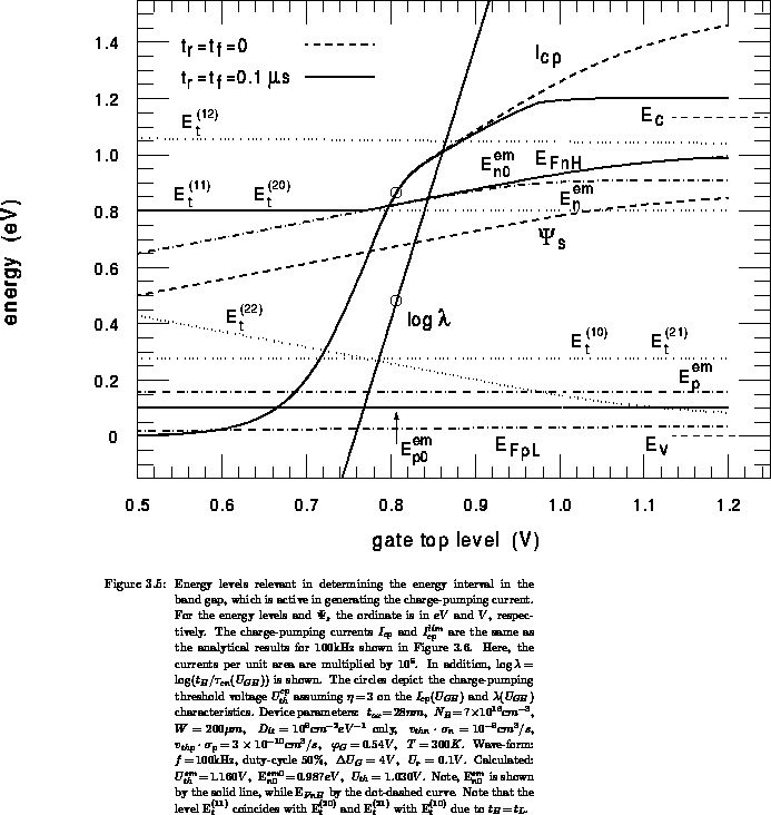
The discussed energy intervals associated with the top and bottom levels and
the pulse edges are shown in Figure 3.5. Moreover, we also
show the scaled and  currents and the parameter
 . To calculate the presented characteristics all
relevant quantities in the MOS structure, like
. To calculate the presented characteristics all
relevant quantities in the MOS structure, like  ,
,  ,
,
 ,
,  ,
,  , are numerically calculated for each
gate top level by using the one-dimensional analytical model described in
Section 2.2. Very low trap density of
, are numerically calculated for each
gate top level by using the one-dimensional analytical model described in
Section 2.2. Very low trap density of
 is assumed to avoid an influence of the charge-potential
feedback effect (the shift on the voltage axis is less than
is assumed to avoid an influence of the charge-potential
feedback effect (the shift on the voltage axis is less than  ), in order
to make the comparison fair. The quantities
), in order
to make the comparison fair. The quantities  ,
,  ,
,
 and
and  are constant and depend on the device
parameters,
are constant and depend on the device
parameters,  and
and  . They are calculated only ones. We have assumed
 and
and  in the calculation of the
non-steady-state emission times.
in the calculation of the
non-steady-state emission times.
A first observation is that the charge-pumping threshold defined
by 3.64 assuming  has a value of
  and lies
significantly below the device threshold
and lies
significantly below the device threshold  . Moreover, the onset
voltage
. Moreover, the onset
voltage  is higher than
  due to a short
  .
Therefore,
.
Therefore,  holds in this case.
The splitting between the levels  and
and  occurs after
  exceeds the threshold
  , because of
 (this fact can be understood by help of
expression 3.67). The splitting between
and takes place when
(this fact can be understood by help of
expression 3.67). The splitting between
and takes place when  .
As interesting, the threshold voltage does not correspond neither
to the beginning of the upper plateau of the curve nor it
relates to
.
As interesting, the threshold voltage does not correspond neither
to the beginning of the upper plateau of the curve nor it
relates to  of the maximal .
The characteristics reflects three specific parts
 ; almost linearly increases in a lin-log scale.
(
; almost linearly increases in a lin-log scale.
( ). The
increases because the active energy interval enlarges with
increasing .
). The
increases because the active energy interval enlarges with
increasing .
 the current is strongly constant and
governed solely by the emission processes at the pulse edges.
the current is strongly constant and
governed solely by the emission processes at the pulse edges.
According to the previous results, two characteristic parts should be recognized
on the rising edge of the characteristics for low pulse
frequencies. There are, however, at least two effects which cause the stretch
out of the rising edge and, eventually, merging of these two parts on the
characteristics of real MOSFETs:
is strongly dependent on the
surface concentration . The fluctuations in the surface
potential cause large fluctuations in the free carrier concentration
 . Thereby, large variations in the contribution to must
be expected across the interface, yielding a stretch-out of the ideal
characteristics, as pointed out in [49].
. Thereby, large variations in the contribution to must
be expected across the interface, yielding a stretch-out of the ideal
characteristics, as pointed out in [49].