We present two contact structures, where a titanium nitride barrier
layer is used to insulate metallurgically the metal from the semiconductor.
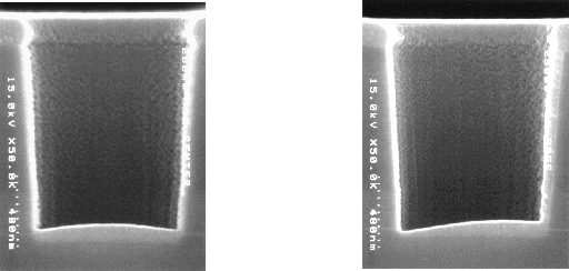
In Figure 7.9 we show SEM pictures after a TiN
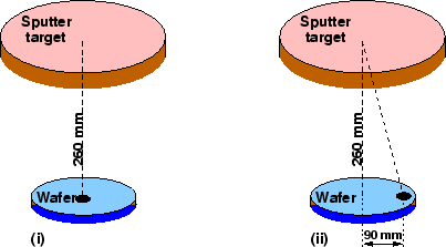
deposition into a 1.0![]() circular hole located 260mm below
the center of the sputter
target disk (see Figure 7.8-(i)) and when the
deposition of TiN is made at a position 90mm off the wafer
center (see Figure 7.8-(ii)). The picturesures in
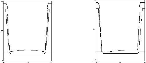
Figure 7.10 are cuts from the simulated three-dimensional
structures and agree well with the upper SEMs.
circular hole located 260mm below
the center of the sputter
target disk (see Figure 7.8-(i)) and when the
deposition of TiN is made at a position 90mm off the wafer
center (see Figure 7.8-(ii)). The picturesures in
Figure 7.10 are cuts from the simulated three-dimensional
structures and agree well with the upper SEMs.
 |
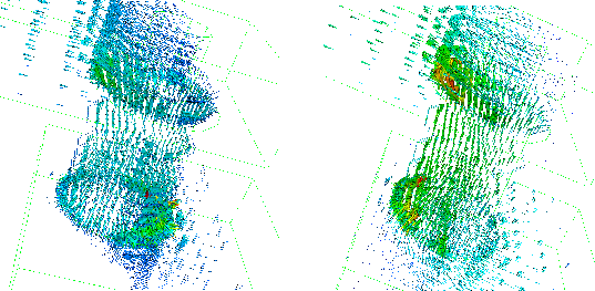
In figure 7.11 we show the current density in the contacts for both cases, after being filled with aluminium. The effect of the asymmetry in the TiN layer in the current density is clearly seen. In case (ii) the current flows mainly in unusual areas, namely in the trailing edge of the contact, whereas in the other case we have the known current crowding effect at the opposite edge.
As electromigration problems are worsened by
current crowding effects [90], our tools can be used to understand
and minimize this unwanted phenomena. The resistance values obtained
were 0.77![]() and 0.89
and 0.89![]() for the upper and lower cases
respectively, and agree well with the experiments.
for the upper and lower cases
respectively, and agree well with the experiments.