Thin films in microelectronics exhibit residual stress which can affect the performance and
reliability of devices. In Chapter 4 it was demonstrated how high values of residual
stress in thin films can be problematic for the mechanical stability of 3D interconnect
structures, such as open TSVs. A high value of residual stress in the W layer of the TSV
structure can increase the probability of delamination at the interface between W and
SiO2.
In this chapter, the mechanism behind stress development during film growth is investigated.
This study is needed for the understanding of the reduction of film stress which is necessary to
increase the mechanical reliability of TSVs. Usually metal films are used in TSVs to
electrically connect the integrated circuit in the 3D structure. Typically, the growth process
of metal films in TSVs follows the Volmer-Weber mechanism. A FEM-based model
describing the stress evolution during the three steps of Volmer-Weber growth was
implemented. In general, stress in the film evolves from compressive to tensile and can
then return to compressive. The stress generated in the film strongly depends on
processing and material properties. Results obtained from the model were compared with
different experimental data. The implemented model helps to predict the intrinsic stress
in thin films during the growth process and enables an analysis of the influence of
fabrication conditions on the thin film stress. The presence of scallops, which appear as a
consequence of deep reactive ion etching, results in reduced intrinsic stress. Film growth
on a scalloped substrate was simulated. When the scallops were more pronounced,
i.e. a larger height/width ratio, the intrinsic stress was further reduced. In addition
film growths at different deposition temperatures and different growth rates were
simulated.
Thin films are utilized in microelectronics to build functional devices such as interconnects. The
properties of a film and its applications are determined by the choice of material and its
geometry. The mechanical properties of thin films with a thickness in the range of
several atomic layers differ from those of bulk materials. These differences are caused
by the diverse microstructures of the film, which depend greatly on the deposition
technique. Most films used for microelectronics are polycrystalline materials composed of
a large number of small crystallites. In order to understand the microstructure of
the film and its mechanical properties, the deposition process must be studied in
detail. Significant stress may develop in the film during the deposition process and
during the subsequent cooling to room temperature, due to a large mismatch in the
thermal expansion coefficients between the material used in the film and the surrounding
layers. Stress can lead to reliability issues such as cracking and delamination within
a device structure, resulting in poor reliability and ultimately early device failure.
Understanding the mechanisms which generate stress in films during the deposition
processes is therefore essential in order to decrease the probability of an interconnect
failure.
In this chapter the intrinsic stress build-up during the deposition process using simulation
methods is analyzed. The deposition process of a given film is modeled by employing
well-established theories and physical models which describe film growth [89, 90, 91, 92]. Each
material has different properties and consequently a different impact on the growth process of
the film. The analysis is focused on W and Cu, which are the materials typically used for TSV
interconnects [28, 29] (Section 1.3.2).
Although this study deals with stress build-up during deposition, for TSVs the
etching step cannot be avoided. In order to fabricate the TSV structure, etching of the
silicon wafer is required. This step can be performed either by ion-enhanced plasma
etching or by deep reactive ion etching (DRIE) [93]. Both methods have their own
reliability concerns: Problems specific to DRIE are scallop formation along the sidewall,
notch formation at the bottom of the TSV, and potential step coverage concerns [94].
Etching using ion-enhanced plasma, such as SF6/O2, results in noticeable sidewall
tapering, resulting in a significant limitation in the aspect ratio of the etched hole
[95].
The mechanical properties of a thin film are highly dependent on the conditions under which the
film deposition takes place. Different deposition processes are used during integrated circuit
fabrication where metals, dielectrics, and semiconductors are grown. Due to thermodynamical
reasons, there are three different modes describing film growth during deposition,
namely Volmer-Weber (V-W), Frank-Van der Merwe, and Stranski-Krastanov [92]. Film
stress development in polycrystalline metal films deposited onto polycrystalline or
amorphous substrates is investigated. The atoms of the polycrystalline metal film are more
strongly bound to each other than to the substrate, and this situation is well described
by the V-W growth mode [42, 90]. The film growth of these materials is therefore
investigated with the basic assumption that the film growth proceeds according to the V-W
mode.
The stress build-up during the growth process is also influenced by the layer on top of which
the deposition takes place, such as SiO2 or the barrier layer. The geometry along the sidewalls of
TSVs on top of which metal liner is deposited can have scalloped features. These features are
a result of the wafer etching process, mainly the deep reactive ion etching (Bosch
process [14, 24]). In this study, the effects of the scallops on the stress build-up during film
growth are also analyzed.
In the fourth processing step (Section 1.3.1) of TSV fabrication a metal film is deposited.
Polycrystalline metal films deposited onto polycrystalline or amorphous substrates are described
by the V-W growth mode [42, 90]. During the V-W mode three unique growth steps can be
distinguished. Each step affects the film microstructure and consequently the physical properties
of the film. The initial stage of film growth is the nucleation of islands onto the substrate.
During the deposition process, atoms arrive on the surface and initiate the nucleation step. The
minimum nucleus, formed by the atoms on the surface, has a characteristic size associated with
a critical initial radius Ri. Beyond this size, the nucleus is stable and begins to grow [90].
The microstructure of a growing film is influenced by the deposition rate vg, the
substrate temperature Ts, and the material properties. Nucleation events continue
to occur during deposition as long as there exists a substrate area exposed to the
atoms [42, 90]. The first growth step consists of the nucleation of islands in the film
deposition process as shown in Figure 5.1 (a). During the second growth step the
islands grow larger in size and start to impinge on each other, forming a continuous
polycrystalline film. This step is commonly referred to as the island coalescence process
(illustrated in Figure 5.1 (b)) After island coalescence film thickening takes place.
In this third step the formed film continues to thicken and gain volume until the deposition
process is interrupted; this step is shown in Figure 5.1 (c)-(d). During the thickening process
the structure of the grains and their evolution are strongly influenced by the adatom diffusivity
of the material employed in the deposition process. There are two different types of
grain-structure evolution. Materials with low adatom mobility (high melting temperature)
exhibit a columnar grain structure with increasing grains during thickening referred to
as Type 1; this type is depicted in Figure 5.1 (c). In these materials (e.g. Si, W,
Fe), the adatom diffusivity is relatively low even at high processing temperature. In
materials with high adatom mobility (low melting temperature), the microstructure
forms equiaxed grains which continue to evolve during film thickening. This process is
typically found in Al, Ag, Au, and Cu, depicted in Figure 5.1 (d), and is referred to as
Type 2.
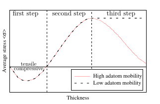
The three V-W growth steps generate stress within the film as shown in Figure 5.2. This
stress evolves from compressive to tensile and can then develop further in one of two different
ways. It can either become compressive again or remain tensile [96], depending on the adatom
mobility of the material used in the deposition process.
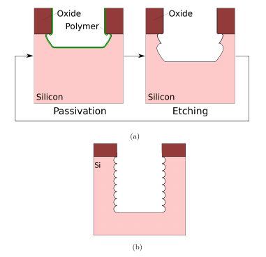
An essential step in TSV fabrication is the etching of silicon, previously described as
the first processing step (Section 1.3.1). Most often this proceeds using DRIE
which is a combination of multiple cycles of the isotropic deposition of a polymer
and an ion-enhanced plasma etching of the polymer and underlying silicon wafer.
The polymer protects the sidewalls from the chemical etch, while it is removed from the
trench bottom. As the bottom becomes exposed, chemical etching proceeds there. This ensures a
vertical etch, but with the presence of a rough, scalloped sidewall. In Figure 5.3 (a) a simple
schematic of the DRIE process is depicted, while Figure 5.3 (b) shows the resulting trench
with scalloped sidewalls after 8 cycles.
The deposition of the thin polymer layer is usually performed in a CxFy gas environment,
while the subsequent etching step is performed in an ion-enhanced plasma environment, usually
using SF6 gas [97]. By controlling the individual times for the deposition and etch steps of
the cycles, the geometry of the resulting scallops can be manipulated. In this work
several scallop structures are examined in order to determine which factors have the
greatest influence on the intrinsic stress generation. With these results the process
sequence proceeds in a way to minimize the resulting stress in the thin film can be
ensured.
During the V-W growth of the film the produced stress plays an important role in the growth
process itself. In the following sections the stress-generation mechanisms is described. First, the
geometric conditions used for the simulation of the growth mechanism, followed by a theoretical
model implemented with the FEM are described.
The model is capable of simulating V-W growth for materials with both high and low
adatom mobility. Although the grain size in films is not uniform, in this work layers
having only a single grain size which corresponds to the average grain size of the
deposited film are considered. This assumption does not correspond to the real condition;
however, a negligible influence of the other grain sizes on the final stress generation is
expected. The main purpose of this study is to analyze the interaction between single
grains.
Further, it is important to note that the crystal orientation, the elastic anisotropy, and the
possible plastic relaxation were not taken into account. These material properties can influence
the stress generation during film growth; however, the intent of the developed model is to
describe qualitative trends of growth in confined geometries and to describe the effects of
fabrication conditions on the stress evolution.
The cylindrical geometry of TSVs could impact and influence the magnitude and
concentration of the film stress. A cause of the complexity to simulate the 3D TSV geometry
only two-dimensional geometries are considered. Further studies are necessary to understand the
impact of the cylindrical geometry of TSV.
The growth process is analyzed for material islands with a hemicylindrical shape [90]. The
material island is represented as a half-cylindrical cut along the z-axis, which lies on a substrate
(Figure 5.4). The length l of the cylinder with a circular-cap cross section is assumed to be
infinite. This assumption is implemented by using the plane strain condition (i.e. strains in
z-direction are zero) in two-dimensional simulations. A thin film as a periodic array of islands is
modeled, and therefore the symmetry boundary condition is imposed on outward normals of the
geometry. A non-slip interface condition between the islands and the substrate is employed. A
schematic representation of the islands is shown in Figure 5.4. FEM model to simulate V-W
film growth is implemented in COMSOL Multiphysics [62] and described in the sections
which follow. A stationary parametric sweep is used to simulate the growth steps.
With the radius parameter R (Figure 5.5) the island geometry is modified as it
grows. At each value of the parameter R a new geometry is created and the stress
generated due to island growth is computed. The stress calculated for every value of R
is used as the initial stress condition (in terms of the stress tensor component σxx
and σyy) for the subsequent simulation step. It is assumed that all materials behave
elastically and that all islands are of the same size. Furthermore, an initial island with a
critical radius (corresponding to a small Ri value) already nucleated on the substrate is
considered. For every simulation step, R is assumed to increase linearly in time t according
to
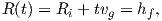 | (5.1) |
where Ri is the initial radius of the island and hf is the film thickness. In this way R
progressively grows as a function of vg.
The average grain size of a film depends on the deposition parameters. In the implemented
model, r is the radius of the island at the coalescence point which corresponds to the average
grain size of the film.
The comparison with experimental data is carried out by computing the average
stress in the film ⟨σxx⟩ using a FEM simulation, followed by the evaluation of the
stress-thickness product ⟨σxx⟩×hf [90]. The stress-thickness product ⟨σxx⟩×hf is often called
the “force/width” and is frequently used in measurements of stresses through thin
films in order to highlight that the stress can have a through-the-thickness variation
which cannot be determined solely by post-deposition curvature measurement [98].
In the first step of V-W growth (cf. Figure 5.1 (a)) a compressive stress develops in the islands
before the film becomes continuous. The stress subsequently emerging is mainly due to the
action of the surface stress [89, 90]. In the solid nucleus the surface atoms have an equilibrium
interatomic spacing which differs from those of the interior (bulk) atoms, due to the
different bondings between surface and interior atoms. This difference in equilibrium
spacing results in the development of surface stress f (cf. Figure 5.5). f is associated
with the reversible work per unit area required to elastically strain a solid surface.
Because of the surface stress f a Laplace pressure ΔP is generated inside the island.
During the deposition process, the island increases in volume dV and some amount
of work ΔPdV is produced. The work available for a volume increase, due to the
pressure, must balance the work required for an increase of the surface, due to the
surface stress f. For positive surface stress f a compressive stress due to Laplace
pressure is present and measurable during the first step of the deposition process. As
for a free surface, surface stress can also be associated with the solid-solid interface
between island and substrate. The interface stress necessary to stretch an interface by
elastically deforming the island and substrate is denoted by g (Figure 5.5) [99].
In this analysis the effect of the stress on the island-substrate interface [89, 90] are
neglected.
There is a second mechanism concurrently generating a compressive stress. This stress is
based on the fact that the island becomes strongly attached (non-slip) to the substrate during
the first growth step. The radius size at which the island is frozen-in at the substrate is denoted
as Rfr which is a function of the strength of the island-substrate bonding. If the radius of
the island is less than Rfr, this mechanism does not affect the internal stress, since
the island is unconstrained [89, 90]. As the volume of the island’s nucleus grows
further, the internal elastic stress tends to relax due to the Laplace pressure. Since
the island is now rigidly bonded to the substrate, the difference between the lattice
parameter, corresponding to Rfr, and the lattice parameter which it would have due to the
Laplace pressure tends to generate a compressive stress in the islands. Considering
both effects and the geometry included in the model, the compressive stress is given
by
 | (5.2) |
This equation is used in the model to describe the initial compressive stress observed at an early
stage of film growth prior to island coalescence.
The tensile stress evolution during film growth is connected to island impingement as depicted
in Figure 5.1 (b). The reason for this process is that the small gaps between adjacent grains
are closed by forming grain boundaries with height hgb (Figure 5.5). The energy
released through the reduction of the surface area of the islands is converted into elastic
deformation energy of the participating grains. In recent years, several approaches for the
computation of the tensile stress generated by island coalescence have been formulated
[90, 100, 101]. In the chosen model’s geometry, the approach described by Seel [90] is
considered, where the generated average tensile stress in the continuous film is given
by
 | (5.3) |
where E is the Young’s modulus, ν is the Poisson’s ratio, γs is the surface energy, γgb is the
grain boundary energy, and r is the radius of the island R at the coalescence point. In the
derivation of (5.3) the islands are considered to have a circular shaped cross section [90]. In this
study (5.3) is used to describe the tensile stress generated during the island coalescence process.
The equation can be applied to predict the average film stress by using parameters γs and γgb
available in the literature [102].
In this section the third growth step for low and high adatom mobility materials is described.
Usually, materials with low adatom mobility exhibit a large tensile stress which remains
constant throughout the thickening process [89, 92]. For these materials, the third step under
the assumption that the stress generated during the second step remains constant throughout is
considered.
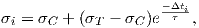
For high adatom mobility materials, on the other hand, compressive stress can re-emerge.
Different theories have been developed to describe compressive stress generation during
the third step of V-W growth. Compressive stress development can be due to the
movement of atoms toward the edges of the film [103], excess adatom concentration
on the surface [104], capillarity effects [105], or movement of atoms into the grain
boundaries [91]. The compressive stress generation by the diffusion of atoms into the grain
boundaries during film growth is considered. This kinetic model for the evolution of
residual stress was validated with measurements in several studies [1, 2, 91]. The
theory assumes that the film during its deposition is composed of multiple thin layers.
The film is thereby represented by parallel atomic layers in the grains with a grain
boundary between them. During the deposition process, the grain boundary height hgb
changes as the atoms fill the edge in between the grains. For this process islands are
considered with circular arcs between the grain boundaries with the same center for all
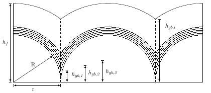
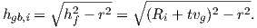
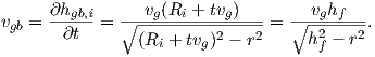
thicknesses as shown in Figure 5.6. hgb,i denotes the grain boundary height, where
the ith layer is grown. The atoms can move into the grain boundary, changing the
grain boundary height from hgb,i to hgb,i+1 [91]. Film stress therefore changes as a
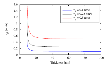
function of the grain boundary velocity vgb. The value of vgb is not constant, as it
does not only depend on the constant growth velocity vg, but also on the geometrical
transformation of the islands. Figure 5.7 shows that a higher vg results in higher grain
boundary velocities and consequently changes the magnitude of the generated compressive
stress due to the shorter time required for the atoms to move into the grain boundary.
The atoms can move into the grain boundary, because the film surface is not in equilibrium
during the deposition process, which leads to an atomic flux. The chemical potentials on the
surface and in the grain boundaries are different from their equilibrium [2, 91].
The increase in the chemical potential on the surface due to non-equilibrium conditions is
defined as δμs. The non-equilibrium condition is caused by the flux of impinging atoms,
leading to a supersaturation of adatoms or to a change in surface morphology. The
non-equilibrium value of the chemical potential in the grain boundary is a cause of the
stress in the layer. It is defined as -σiΩ where σi is the stress in the ith layer and
Ω is the atomic volume. The chemical potential is negative, because the chemical
potential is lower than the equilibrium value in the presence of tensile stress. The
stress in the layer, and therefore the chemical potential in the grain boundary, changes
with time due to the diffusion of atoms into the grain boundary. The difference in
the chemical potential between the surface μs and the grain boundary μgb is given
by
 | (5.4) |
The chemical potential depends on growth conditions and on the stress in the film. The
difference in the chemical potential Δμ is the driving force behind the necessary movement of
atoms Ngb from the surface to the grain boundary. When there is no growth, the chemical
potential on the surface and at the grain boundary are identical, therefore no atom moves into
the grain boundary. The rate of insertion of atoms into the grain boundary is defined as
[1, 2, 91]
 | (5.5) |
where Cs is the fractional coverage, D is the effective diffusivity, a is the height of an atomic
step (Ω1∕3), k is the Boltzmann constant, and T is the deposition temperature. The atomic step
is the amount of space necessary to close two adjacent layers, forming a bond and an
additional grain boundary. The atoms can only migrate after a grain boundary is
formed, after which a tensile stress, generated by the island coalescence process, is
already present. The insertion of atoms into the grain boundary decreases the tensile
stress in the film. Thus, the generated stress σi at the ith layer can be described as
[1, 2]
 | (5.6) |
where σT is the tensile stress generated due to island coalescence, ν is the Poisson ratio, and L is
the grain size (equal to 2 ⋅r (cf. Figure 5.5)). The second term in the right-hand-side of (5.6)
represents the compressive stress generated by the movement of atoms into the grain
boundary.
The stress evolution for the ith layer is obtained by differentiating (5.6) with respect to time.
Using (5.5), the rate of stress change is given by
 | (5.7) |
By solving (5.7), Chason et al. [1, 2] evaluated the stress in the ith layer to
 | (5.8) |
where Δti is the time period in which the atoms can move into the grain boundary. The other
terms are defined as
σ
c
=
-
 ,
,
| (5.9a) |
 = =  . . |
(5.9b) |
The time increment Δti is defined [1, 2] by
 | (5.10) |
When the layer forms (t = ti), only the term σT , which is due to coalescence, is relevant.
The velocity vgb has an important influence on compressive stress release. At the beginning,
vgb is high and the atoms have a short time in which to migrate into the grain boundary. The
stress in the layer therefore becomes more tensile. When the thickness increases, vgb decreases
and converges to the average deposition rate; consequently the tensile stress in the film
decreases.
To include (5.8) in the model, a reformulation is performed. The velocity vgb can be obtained
from the geometry; therefore, the stress for discrete layers can be replaced by a continuum
description. By using (5.1), the term hgb,i can be written as:
 | (5.11) |
The grain boundary velocity is given by
 | (5.12) |
In [1, 2] the stress-thickness product of the film was calculated by summing the stress
contributions from each layer and multiplying by the layer thickness
![Nla∑yers[ -Δti]
⟨σ⟩hf = a σC + (σT - σC )e -τ--.
i=1](Main1024x.png) | (5.13) |
In this model the average stress is calculated as a function of film thickness hf with (5.8) and
(5.12) integrating over the interval [hgb,1,hgb,i]
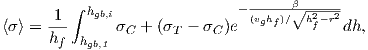 | (5.14) |
where
 | (5.15) |
The parameter β has the dimension of a velocity, and its value influences the exponential term
in (5.14). The average stress generated in the film depends on the number of mobile atoms
adjusted by the parameters β and vg. The value σT can be calculated theoretically using
the stress generated at the coalescence point [90] or by fitting to experimental data
[1, 2].
Equation (5.14) is implemented in the model and enables to simulate growth processes for
different boundary conditions. At every film thickness the integral (5.14) is calculated and its
value is used as the initial stress in the film for the next simulation step. Using experimental
data, the model can be calibrated and evaluated for different boundary and geometric
conditions.
W and Cu are materials frequently used for TSV interconnects [28, 29]. W is a material with a
low adatom mobility, and it exhibits a high value of intrinsic tensile stress. Cu is a material with
high adatom mobility and can exhibits compressive or tensile stress depending on the film
thickness and the conditions of deposition. For open TSVs, W [29] or Cu [28] are usually used
for metalization.
The development of compressive or tensile stress in the thin film in an open TSV can induce
delamination or cracking (Chapter 4). Usually, tensile stress can generate surface
cracking, channeling, spalling, and debonding of the substrate. If the stress in the
film is compressive, the dominant failure modes are buckling-driven interface or edge
delamination [45]. In the following sections an investigation of the factors which influence the
evolution of stress in the film in order to ascertain how to reduce the probability of
mechanical failure is studied. The capabilities of the model are demonstrated for W and Cu
films.
As described in Section 5.2.1 during the first step and the second step of the V-W growth,
materials with low and high adatom mobility exhibit the same physical behavior. Therefore, it is
important to clarify that in this work the results regarding the first and second step are valid for
both types of materials. A complete analysis of the three steps of the V-W for low
adatom mobility is reported. In contrast only the third step of the V-W for high
adatom mobility is presented, since the first two steps are identical to the low adatom
mobility. During these two steps proper material parameters have to be used in (5.2) and
(5.3) [89, 90].
In the following sections the mechanical effects of the V-W growth on a full plate sample and at
the sidewall area of an open TSV structure are examined.
Residual stress measurements of W layers, either deposited as blanket films or grown along
the sidewall of TSVs etched in silicon, were investigated in [86]. In the full plate sample
described in [86], a specific stack was deposited on the silicon substrate. The stack was
composed of SiO2 (500 nm), Ti (40 nm), TiN (55 nm) and W (200 nm). The layer sequence of
Ti/TiN/W was repeated twice. In the W layer on the top of the sample structure a grain size of
300 nm (2⋅r in Figure 5.5) was measured. Since the V-W growth impacts mainly only
the first layers, the implement model was simplified by considering one Ti/TiN/W
stack.
For the full plate sample the residual stress measured [86] at room temperature was
1.6 GPa. In the TSV sidewall it was four times smaller 0.4 GPa. This large difference could be
caused by delamination, difference in the residual stress, non equi-biaxial state of stress or by
the presence of rippled sidewalls in the TSV [86]. The measured residual stress is basically
thermal stress generated from the different thermal expansion coefficients between film and
substrate (cf. Section 2.3.2). The V-W growth occurs during the deposition process where the
film stress is different than the value measured at room temperature. Therefore, a FEM elastic
thermo-mechanical simulation was performed to obtain the value of intrinsic stress during the
deposition process. By considering a deposition process at 400 ∘C, the obtained film
stress was 0.64 GPa. In the following simulations the calibration of the full plate
sample with a grain size of 300 nm was performed by using an intrinsic film stress of
0.64 GPa.
During the first step of the V-W growth (5.2) was applied to simulate the growth of W islands
already nucleated on a Ti/TiN substrate.
The stress σxx distribution due to the Laplace pressure during the first step of the V-W
growth is shown in Figure 5.8. A low tensile stress acts on the surface of the islands and a
compressive stress at the center of the islands.
The islands exhibit a compressive average stress ⟨σxx⟩ (negative value) which is
reported as a function of the film thickness in Figure 5.9 for different grain sizes. The
magnitude of the generated stress is influenced by the grain sizes of the islands. Thin films
having big grain size produce less compressive stress compared to small grain size.
Because Rfr=10 nm was set the compressive stress starts from the thickness of 10 nm
(cf. Figure 5.9).
The generated stress during this first step of the V-W growth can influence the substrate
(Figure 5.8). If the substrate is thin and the generated stress is high, the probability of crack
or delamination at the interface increases (Chapter 4).
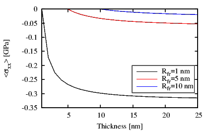
Rfr is a function of the strength of the island-substrate bonding and in this configuration it
was assumed to be in a range between 1 nm and 10 nm [90]. In Figure 5.10 results for three
different Rfr values and an island grain size of 300 nm are shown. The compressive stress
decreases with increasing Rfr, and the smallest Rfr produces a compressive stress around
300 MPa. Stress in this range can influence the mechanical stability of the system and in
particular in the thin layers.
The magnitude of the generated compressive stress is determined by the surface stress f, the
frozen-in radius Rfr, and the island radius R. Due to the simulation conditions, islands having a
large grain size do not impinge rapidly. At the initial simulation step, the distance between
islands corresponds at the simulated grain size (2 ⋅r in Figure 5.5). When a large grain size is
considered, the initial distance between islands is wide. Therefore, islands of a depositing film
whose expected grain size is large do not impinge rapidly. The substrate is therefore exposed to
compressive stress for an extended period of time. If Rfr is small, the strength of the
island-substrate bonding is strong and compressive stress can reach a high value, critical to the
mechanical stability of the system. In this study the model was applied for a low
adatom mobility material. It should be clarified that the model can also be adapted
to suit high adatom mobility materials by adjusting the parameters f and Rfr in
(5.2).
During the coalescence process the film stress is gradually changing from compressive to tensile.
(5.3) was used at the first contact point between islands where the tensile stress is generated due
to the impinge of them. During the coalescence process grain boundaries are formed due to the
reduction of the surface area of the islands.
The simulation was calibrated by using the intrinsic stress value of 0.64 GPa
(cf. Section 5.4.1.1). The term (2γs-γgb) in (5.3) was varied until the desired average ⟨σxx⟩ at
the film thickness of 200 nm was obtained. The values used are shown in Table 5.1.
|
|
|
| f [J/m2] | Rfr [nm] | (2γs- γgb) [J/m2] |
|
|
|
| 2.833 [99] | 10 | 7.6 |
|
|
|
| |
Table 5.1: Parameters used for the simulations. The value (2γs - γgb) was used as fitting
parameter.
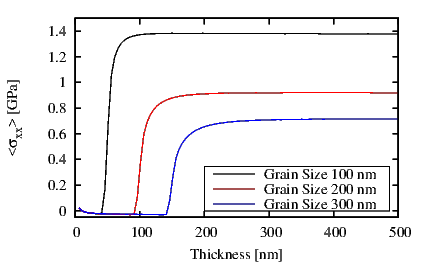
The film stress ⟨σxx⟩ as a function of the film thickness is shown in Figure 5.11. The
simulations were carried out until a thickness of 500 nm was reached. Initially, the film stress is
compressive when coalescence starts the compressive stress decreases until it changes its sign
and becomes tensile. Subsequently, the film stress increases until it saturates and
reaches a constant value. The end of the coalescence process corresponds to the first
peak value of the tensile stress. In Figure 5.11 the influence of the grain size on
the film stress is reported. Small grain size produces high stress in the film, on the
other hand big grain size produces a small film stress [90] as described in Section
5.3.3.
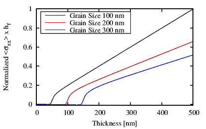
The stress-thickness ⟨σxx⟩× hf is mainly tensile and increases nearly linearly with film
thickness. The normalized stress-thickness for different grain size is displayed in Figure 5.12.
The constant slopes for thicknesses above 50 nm (grain size=50 nm), 100 nm (grain size=100
nm), and 150 nm (grain size=150 nm) indicate the independence of the film stress on the film
thickness.
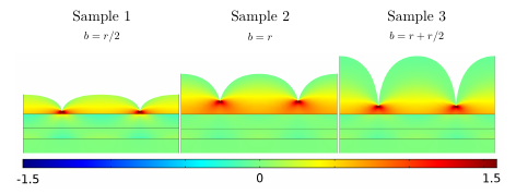
The island coalescence process assuming three different nuclei shapes was investigated.
In this analysis, stress forms in the film due only to the island coalescence process.
The three samples studied are shown in Figure 5.13. Sample 2 shows an island with a
circular shape, whereas Sample 1 and Sample 3 depict islands of elliptical shape. The island
height b is a function of the grain radius (cf. Figure 5.5). For all three samples (5.3)
was applied at the first contact point between the islands. With the exception of
the grain height, all parameters were kept constant for the simulations of all three
samples.
The difference in island geometries leads to a different stress evolution during V-W growth.
Figure 5.13 shows the stress components σxx generated, when coalescence takes place. Due to
the different height to width ratio, coalescence is initiated at different film thicknesses. The
stress increase associated with film coalescence therefore starts at different times for Sample 1, 2,
and 3 (Figure 5.14).
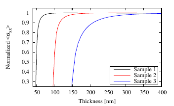
When the film converges to a homogeneous height, the surface irregularity reduces, and the
islands’ initial shapes have no influence on the intrinsic stress in the film. This phenomenon can
be observed in Figure 5.14, where the normalized average stress ⟨σxx⟩ as a function of film
thickness is shown to be constant after film coalescence and equal for all three island
shapes.
The maximum stress develops in the film, when the surface roughness is low, specifically
when the grain boundary height is equal to the film thickness of a homogeneous film. During the
film growth after island collision, the grain boundary height changes as the film thickness
increases (hgb in Figure 5.6). At the point of coalescence between islands the grain boundary
height is small, but as the film becomes thicker the grain boundary height grows
reaching approximately the film thickness. Tensile stress develops due to a reduction in
the surface areas of the islands [90, 100, 101] and the maximum tensile stress is
generated when the grain boundary height is equal to the film thickness. This process is
consistent with the results reported in [106], which suggests that tensile stress due to
coalescence evolves during grain boundary formation and reaches its maximum value, when
the film develops into a homogeneous film. From this analysis, it is possible to see
how the microstructure influences ⟨σxx⟩ at different film thicknesses. In particular,
the grains’ size influences stress as well as the thickness of the film and the islands’
shapes.
For low adatom mobility materials the stress generated at the end of the coalescence process
remains constant during the third step of V-W growth. The model was verified for W V-W
growth on a full plate sample and at the sidewall of an open TSV. The V-W growth simulation
of W on a full plate sample was calibrated using corresponding experimental results Section
5.4.1.1. Subsequently, the calibrated model was used to simulate the V-W growth of W at the
sidewall of an open TSV.
The third simulation step is dominated by the film-thickening. The deposited metal (W) is a
low-mobility material, therefore the generated intrinsic stress remains tensile during the
growth [89]. In Figure 5.11 the results of the V-W growth on a full plate sample are
shown. The mechanical stress in the film is constant and tensile after the end of the
coalescence process. As the grain size of the film decreases the intrinsic film stress
increases.
The formation of surface roughness along the TSV sidewall, called scallops, due to the
etch process is characteristic of open TSVs. This particular structure modifies the
distribution of stress in the W layer. The CVD growth process was reproduced on a
scalloped surface. As reported in [86] the film stress measured at room temperature
along the sidewall of an open TSV was four times smaller than the stress in a full
plate sample. To understand the possible effects of the TSV geometry a more detailed
investigation on the influence of a scalloped substrate on the intrinsic film stress was carried
out.
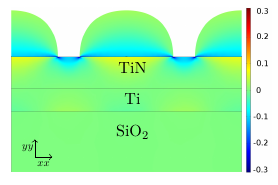
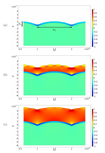
In Figure 5.15 the 1 μm/0.1 μm structure is depicted, where ws and hs indicate the width
and the height of the scallops, respectively. The W layer is grown on top of a 40 nm TiN layer
which sits on top of a SiO2 substrate; this structure corresponds to the sidewall of an open TSV
before W deposition [29]. During V-W growth the generated stress also influences the substrate
where the thin film is grown. In order to investigate how the mechanical stress affects the
substrate, a compressive residual stress of 1GPa was set in the TiN layer [67]. Usually the
SiO2 substrate contains inconsequential amounts of residual stress [67] and it was
therefore considered stress free in this study. In all simulations the same material
properties were used and the grain size of the W islands 2 ⋅ r was set to 200 nm.
The W layer exhibits a low adatom mobility; therefore (5.3) was used to describe the film
growth. The effects of the scalloped structure on the normalized average stress were investigated
(cf. Figure 5.15). This particular structure can produce a high concentration of stress during
film thickening, which leads to mechanical failure. In Figure 5.15 the normalized stress
distributions at film thicknesses of ~0 nm, 200 nm, and 400 nm are displayed. The
highest tensile stress is observed at the intersection points of the grains. In turn,
the highest compressive stress is observed at the intersection points of the scallops.
These locations are the critical areas in which a crack in the film or delamination can
occur.
The compressive stress in the TiN layer is influenced by the film growth. Initially high values
of compressive stress are concentrated only at the intersection points of the scallops. However,
when the film is formed, the compressive stress in the TiN layer spreads toward the center of the
scallops.
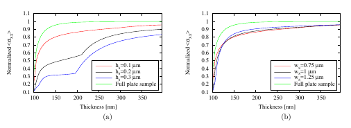
By simulating different scallop sizes important information about the stress generation during
film growth on a confined geometry was obtained. The etch process can be designed in order to
produce scallops with different geometries. Scallops with a width/height of 0.75 μm / 0.1 μm,
1 μm / 0.2 μm, and 1.25 μm/0.3 μm were considered. As previously reported the average film
stress is strongly dependent on the film thickness. In the scalloped structure, compared to the
full plate sample, the tensile stress due to coalescence increases at a reduced rate as the
thickness increases.
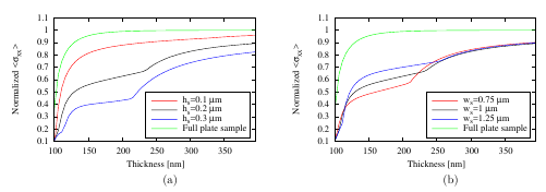
Figure 5.16, Figure 5.17, and Figure 5.18, are the simulation results of a W film grown
on scalloped geometries with height/width of 0.75 μm/0.1 μm, 1 μm/0.2 μm, and
1.25 μm/0.3 μm, respectively. In all the figures the green line indicates the normalized
average stress during the V-W growth on a full plate sample. The other lines represent
the normalized average stress during V-W growth for different scalloped structures
where hs and ws were varied. For the full plate sample, during the third V-W growth
step, the average stress remains constant, as is characteristic of low adatom mobility
materials.
In Figure 5.16 (a), Figure 5.17 (a) and Figure 5.18 (a) the width ws of the scallops
was kept constant at 0.75 μm, 1 μm, and 1.25 μm, respectively, and the height hs of the
scallops was varied between 0.1 μm, 0.2 μm, and 0.3 μm at every width. In all samples the
same stress evolution is observable. The width ws of the scallops influences the stress at small
thicknesses; subsequently, as the thickness increases, the film stress evolves similarly for all
samples. In Figure 5.16 (a) it is evident that the width of the scallops affects the film stress
evolution until a thickness around 200 nm is reached. Similar is the case in Figure 5.17 (a)
and in Figure 5.18 (a), where the film stress evolution is unaffected by scallops
until thicknesses of 225 nm and 250 nm are reached, respectively. In all figures it is
evident that a sharp stress increase takes place during thickening. This increase is
connected to the overtaking of grains by neighboring grains. As the scallop width ws
increases this process is delayed, leading to the sharp stress increase at different film
thicknesses. This phenomenon of overtaking grains is further described in the next
subsection.
In all the samples with hs=0.1 μm and a varied ws the normalized average stress does not
significantly vary with the scallop width. This is depicted in Figure 5.16 (b), where in all the
scalloped structures the tensile stress evolves similarly and converges at the same maximum
value for all samples. In this configuration the scallop heights do not significantly change the
film geometry which is still essentially flat and therefore no extreme stress variations are
observable.
In Figure 5.17 (b) hs was set to 0.2 μm and ws was varied. Here, between film thicknesses
of 125 nm to 250 nm different stress behaviors are observed. In this thickness range the film
assumes the scalloped shape and its stress is influenced by the geometry. In all the results a
sharp stress increase is evident due to grains which are overtaken by neighboring grains. The
smallest generated stress is in the structure having ws=0.75 μm due to the scallop curvatures. In
general, as the curvature of the scallops increases (big hs and small ws), the film stress
decreases.
In Figure 5.18 (b) the scallop structures have hs=0.3 μm and the width ws was
varied. These samples correspond to the structures having the most curved scallops. In
particular the sample with ws=0.75 μm has the most pronounced scallop curvature and a
small average film stress develops before finally reaching the maximum stress. Also
here the sharp stress increase at a thickness between 200 nm and 250 nm is due to
the overtaking of grains by neighboring grains. This stress behavior is related to the
curvature of the scallops that influence the grain growth during film thickening. The
grain boundary height hgb increases slowly, unlike in a full plate sample. During the
deposition process the film stress build-up evolves. The maximum tensile stress is reached
only when the grain boundary height is equal to the film thickness [106]. Due to the
scallop curvatures a homogeneous film (for low roughness the grain boundary height
corresponds to the film thickness) is formed at high thicknesses; therefore, at small
thicknesses the grain boundary height is small and a low amount of intrinsic tensile stress is
generated.
In all samples a stress decrease was observed for thin films (below ~200-250 nm), when a
notable curvature is present in the scallops, such as at high hs or at small ws. The generated
stress in these samples is less than that produced in a full plate sample. When the grains
are grown on curved surfaces, they have less contact area, thereby producing less
stress.
This simulation approach can be used to investigate the stress evolution for arbitrary
geometries.
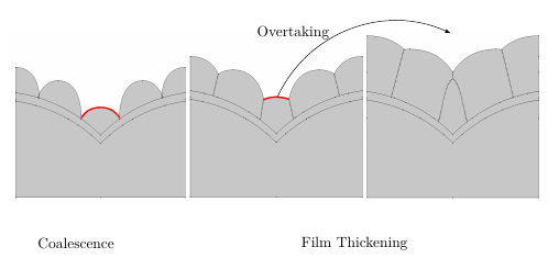
The sharp stress increase observed in Figure 5.16, Figure 5.17, and Figure 5.18 of the
previously subsection can be described by considering the overtaking of grains. As the film
thickness increases a grain can be overtaken by the neighboring grains as depicted in
Figure 5.19. As described previously the intrinsic stress build-up is an evolving process
dependent on the grain boundary height. During overtaking the contact area (grain boundary
height) between grains rapidly increases and the film starts to be homogeneous, leading to a
rapid stress increase.
The stress in low adatom mobility films grown on a full plate sample stays constant during
the third step of the V-W growth. However, when films are grown on a scalloped structure
this is no longer the case and two phases of film thickening can be clearly identified:
- The first phase identifies the stage before the overtaking of grains. The film stress
has a small value compared to a film grown on a full plate sample. In this phase
the intrinsic stress is significantly lower than that in flat samples. This explains the
reduced stress in thin films from published experiments [86].
- The second phase indicates the stage after the overtaking of grains. A homogeneous
film is forming and a rapid stress increase in the film increase characterizes this stage
is observed. As thickening proceeds, the stress approaches the value found in flat
samples.
The two-phase stress development during thickening suggests that the scallops only help reduce
stress in thin films. For thick films the stress eventually reaches the levels observed in flat
samples.
The implemented model, which simulates the generation of compressive stress during the third
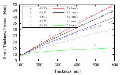
V-W growth step for high adatom mobility materials, was verified by using stress measurements
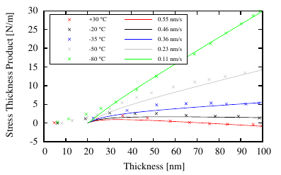
of Ag films grown on SiO2. In [1, 2] the stress-thickness product as a function of thickness was
measured by changing the deposition temperature. Since the adatom mobility depends on
temperature, the shape of the curve at higher temperatures becomes less tensile (i.e. more
compressive) as the thickness increases. This experimentally derived behavior [1, 2] is
shown in Figure 5.20. All samples were grown using a fixed growth rate of vg = 0.2
nm∕s.
With the FEM model the experimental data were reproduced by using (5.14),
where σT = 1550 MPa and σC = -200 MPa. All simulations were started with an
assumed film thickness of 20 nm. The model reproduces the experimental results
at different temperatures by varying β (the employed β values are in the inset of
Figure 5.20).
In the stress-thickness versus thickness plot (cf. Figure 5.20) a tensile behavior is only
observable at low temperatures (green line), and at high temperatures the transition from tensile
to compressive stress can be seen clearly (red line). In these simulations is assumed that the
generated compressive stress is driven only by adatom mobility, allowing the atom to move into
the grain boundary. This suggests to vary the atom diffusivity with β. Higher values of β
correspond to higher adatom mobilities, whereas smaller values stand for lower adatom
mobilities. The simulations produced results with qualitatively good agreement to
experimental data and it provided an understanding of the transition from tensile to
compressive stress. The best fittings are obtained at low deposition temperatures. This
observation is ascribed to a constant distribution of grain sizes under these growth
conditions. At higher temperatures the simulation results of the model fit quantitatively
better to experimental results at high film thickness. Especially for temperatures
between -20 ∘C and 30 ∘C (cf. black and red lines in Figure 5.20) the simulations
are in quantitatively good agreement for thicker films, where the model predicts the
generation of compressive stress. For small thicknesses the model underestimates the
generation of tensile stress. It is supposed that the film roughness and the different sizes
of the islands for small film thicknesses have a significant influence on the stress.
These effects are not included in the model, due to the impossibility of tracking them
experimentally.
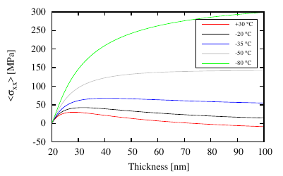
⟨σxx⟩ was calculated in the film as a function of film thickness and the results are depicted in
Figure 5.21. The magnitude of the stress is strongly dependent on the deposition
temperature. The transition from tensile to compressive stress at high temperatures is clearly
observable. Therefore, the model can be used for the simulation at different deposition
temperatures.
As far as interconnect design is concerned, the knowledge of ⟨σxx⟩ as function of film
thickness can be used to reduce the probability of mechanical failure. In this study the
capability of the model to reproduce the deposition process for different temperatures were
verified.
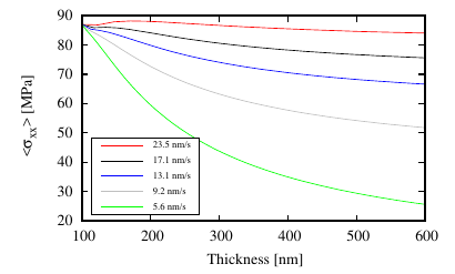
In [3] stress measurements during Cu electrodeposition on an Au substrate were carried out. Cu
was deposited at room temperature with different growth rates vg. In order to create a
consistent starting layer with respect to grain size for all the considered deposition processes,
100 nm of Cu was deposited with a growth rate of 9.1 nm∕s in the first phase. The resulting
grains had an average size of L = 200 nm [3]. After reaching 100 nm thickness, the
second phase was initiated by changing the electrical potential, thereby producing
different growth rates. Unlike the situation described in the previous section, the model
applied here was verified by changing the growth rate and keeping the other parameters
constant.
The electrical potential at the electrodes influences the nucleation density and the growth
rate in the electrodeposition process.
The experimental stress-thickness product as a function of thickness was reproduced by
simulation. The parameters σT = 230 MPa, σc = -195 MPa, and β = 4.125 nm∕s were utilized
in the simulation. In Figure 5.22, the obtained experimental values for the stress-thickness
product between -0.45 V to -0.65 V were compared with the simulation results. An average
grain size of 200 nm was used as it fits well to experimental data, even though the grain size for
thicknesses over 100 nm was not measured for this experiment [3]. A change in the average grain
size during growth may alter the film stress, however, the model qualitatively reproduces the
experimental results well with the assumed grain size. The model accurately fits the
experimental results for growth rates between 9.1 and 23.5 nm∕s. For this range of deposition
rates the grain sizes generated by the initial deposition process for all samples were
kept constant in the subsequent process phases as the growth rates are increased. At
a growth rate of 5.6 nm∕s the model does not properly predict the stress for high
material thicknesses possibly due the fact that the growth rate in the initial phase
surpasses the growth rate of the thickening phase. This can lead to the generation
of additional grains leading to a higher roughness of the film. These effects, which
might influence the stress in the film, are not included in the model. The growth
rate has a significant influence on the residual stress in the film (cf. Figure 5.23).
For all the simulated deposition conditions, as the growth rate decreases, the film
stress reduces. Slow growth rates correpond to a low grain boundary velocity and
therefore the film stress becomes less tensile and more compressive. At slow growth rates
the adatoms have ample opportunity to move into the grain boundary, generating
compressive stress, while at high growth rates the stress remains almost constant throughout
thickening.
The intrinsic stress generated during the deposition processes of thin metal films was
investigated. Since the metalization of wafers in microelectronics is usually performed at the
"back end" of the production line, it is important to understand the origin and behavior of stress
during film deposition in order to increase reliability and to prevent mechanical failure of the
interconnects. The three growth steps responsible for the evolution of stress were identified, and
each of them was simulated by FEM.
By applying the concepts of Laplace pressure and of the frozen-in radius, compressive stress
generation in the islands during the first growth step was simulated. The estimation of the
magnitude of the stress is a very challenging task due to the lack of experimentally confirmed
parameters. Nevertheless, the model helps to understand, how stress caused by volume increase
develops at the substrate and inside the islands. Information regarding stress distribution in the
substrate is useful, when it comes to adjusting the deposition process in order to limit
mechanical failures (e.g. delamination, cracks, etc.).
By using Seel’s approach the second step regarding the process of island coalescence was
examined. At small thicknesses of the film, the shape of the island, grain sizes, and film
roughness are factors which influence the stress build-up in a film. For thick films the film is
homogeneous (low roughness) and the stress is equally distributed. During the growth
process, the maximum stress is reached, when a homogeneous film is formed. For a
thin film the island shapes change the stress distribution and thereby the average
stress in the film. Therefore, different stress values can be obtained in thin films.
Smaller grains exhibit higher stresses, whereas bigger grains produce lower stress in the
film.
The stress behavior due to low adatom mobility was analyzed during W growth on a
scalloped structure and on a full plate sample. The results demonstrated that the substrate
shape influences the film stress for thin films. Thin films grown on a scalloped surface with a
high curvature develop a small intrinsic stress. Due to the curved substrate the thickness
necessary to reach a homogeneous film increases leading to a small intrinsic stress generation.
The grain boundary height on a scalloped structure grows differently than in a flat sample.
During the film grows, height and width of the scallops influence the contact areas
between islands and consequently the tensile stress generated. As film thickness increases
the film becomes homogeneous (when the grain boundary height correspond to film
thickness) and the tensile stress converges at the stress value found in a full plate. A
new phase in the stress evolution during film thickening on scalloped surfaces was
identified. The first phase indicates thin film growth at the stage before the overtaking of
grains, while the second phase occurs after grain overtaking and is similar to the
traditional V-W thickening during deposition on flat surfaces. This information can be
used during deep reactive ion etching for TSV fabrication. By controlling the etching
parameters, the appropriate scallop size necessary to minimize mechanical failure
can be achieved. Scallops having a larger height/width ratio induce small intrinsic
stress generation. The scallop geometry permits to reduce considerably the film stress.
Deposition on scallops having the largest height/width ratio (hs=0.3 μm / ws=0.75
μm) produce ~70% less film stress compared to a full plate sample. On the other
hand, films grown on scallops having the smallest height/width ratio (hs=0.1 μm /
ws=1.25 μm) produce ~20% less of stress compared to a full plate sample. Scallops
influence the stress evolution between the coalescence process and the overtaking of
islands. As the film becomes thicker the scallop geometry does not impact the stress
evolution.
A high adatom mobility model was implemented on the basis of the theory described by
Chason. Compressive stress in a film is generated due to the movement of atoms into the grain
boundary. The implemented model is able to reproduce measured data from two different
experiments. In the first, the effects of the deposition temperature on film stress and in the
second the effects of different growth rates were replicated. High deposition temperatures and
slow growth rate produce small intrinsic tensile stress. The calibrated model can be applied
to investigate the stress evolution for future applications. In open TSVs, Cu is still
deposited by electrodeposition. This process often shows an abnormal grain growth. For
such cases the described model is not able to properly handle the deposition process.
Future technologies generations demanding higher aspect ratio TSVs might require
a CVD Cu deposition. However, Cu films deposited by CVD are still not worthy
manufacturing [107].