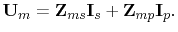
The relation of the port voltages to the port currents is given by the impedance matrix
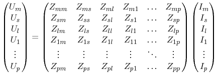 |
(7.39) |
where indexes  ,
,  , and
, and  are assigned to a measurement port, a port at the source
position of a trace inside the enclosure, and a port at the load position of this trace,
respectively. The indices
are assigned to a measurement port, a port at the source
position of a trace inside the enclosure, and a port at the load position of this trace,
respectively. The indices  to
to  are assigned to the interface ports at the slot of
the enclosure. The elements of the impedance matrix are calculated analytically
with (7.14) for a slim (
are assigned to the interface ports at the slot of
the enclosure. The elements of the impedance matrix are calculated analytically
with (7.14) for a slim (
 ) rectangular enclosure with a
slot on one edge. With
) rectangular enclosure with a
slot on one edge. With  at the voltage measurement port,
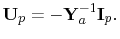
matrix (7.39) is separated to the slot port matrix
equation
at the voltage measurement port,
matrix (7.39) is separated to the slot port matrix
equation
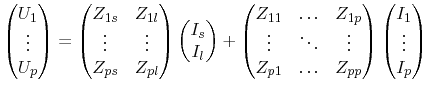 |
(7.40) |
with the matrix notation
 |
(7.41) |
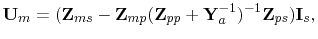
and the measurement port matrix equation
 |
(7.42) |
with the matrix notation
 |
(7.43) |
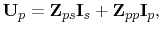
The admittance matrix
 with the elements
from (7.38) relates the voltage vector
with the elements
from (7.38) relates the voltage vector
 to the the current vector
 at the interface ports with
 |
(7.44) |
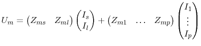
This leads to the final formulation for the voltage on the test port
 |
(7.45) |
and the voltages on the interface ports
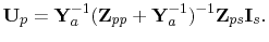 |
(7.46) |
When the radiation loss becomes very low,
is almost singular. For a
nearly singular
, (7.45) can be
simplified to
 |
(7.47) |
and (7.46) to
 |
(7.48) |
to avoid matrix inversion in such a case.
Since (7.47)
and (7.48) neglect the radiation loss, these
equations may only be used at frequencies, where
is nearly
singular.
The internal enclosure voltages and the slot voltages between the metallic
cover and bottom plane are modeled accurately
with (7.45), (7.46),
(7.47),
and (7.48). With the voltages at the
slot (7.32)
and (7.33) the free space far field radiation from the
enclosure slot can be calculated analytically. This model enables efficient, quantitative
investigations in the predesign phase of a device, especially regarding placement
decisions. Design rules, derived from the discussion of the analytical cavity model in
Section 5.8 and
Subsection 7.1.3 are investigated in
Chapter 8 regarding their quantitative relevance in the radiated
far field.
C. Poschalko: The Simulation of Emission from Printed Circuit Boards under a Metallic Cover