previous up next contents
Prev: 5.2.1 Multiple Gaussian Peaks Up: 5.2 Benchmarks Next: 5.2.3 Phase Shifted Outriggers


5.2.2 Reflective Notching

The second example includes standing waves and reflection at a defect inside the resist. The defect works as reflecting plane at an angle of 22.5$^\circ$. The overall intensity distribution is composed by four beams. Beam1 is a vertical beam with standing waves directed towards the defect, thus forming a reflected beam at an angle of 45$^\circ$ which mirrors the standing waves from the incident beam. The reflected beam is given by Beam2. A second vertical beam is composed by the phase shifted Beam3 and Beam4, respectively. This beam is far enough away from the defect and therefore not reflected. The complete set of equations is
$\displaystyle \mathrm{Mag_1^0}$ $\textstyle =$ $\displaystyle 1.0*\exp\{-0.01*[(x-20)^2+(y-40)^2]\}$  
$\displaystyle \mathrm{Mag_2^0}$ $\textstyle =$ $\displaystyle 0.5*\exp\{-0.01*[(x-z)^2+(y-40)^2]\}$  
$\displaystyle \mathrm{Mag_1}$ $\textstyle =$ $\displaystyle \left\{\begin{array}{r@{\quad:\quad}l}
\mathrm{Mag_1^0} & 0.4142*x+z > 27.653\\
0 & 0.4142*x+z \le 27.653
\end{array}\right.$  
$\displaystyle \mathrm{Mag_2}$ $\textstyle =$ $\displaystyle \left\{\begin{array}{r@{\quad:\quad}l}
\mathrm{Mag_2^0} & 0.4142*x+z > 27.653\\
0 & 0.4142*x+z \le 27.653
\end{array}\right.$  
$\displaystyle \mathrm{Mag_3}$ $\textstyle =$ $\displaystyle 1.0*\exp\{-0.01*[(x-80)^2+(y-40)^2]\}$  
$\displaystyle \mathrm{Mag_4}$ $\textstyle =$ $\displaystyle 0.1*\exp\{-0.01*[(x-80)^2+(y-40)^2]\}$  
$\displaystyle \mathrm{Pha_1}$ $\textstyle =$ $\displaystyle \sin(\pi*z/10))$  
$\displaystyle \mathrm{Pha_2}$ $\textstyle =$ $\displaystyle \sin[(40-x-z)*\pi/(10*\sqrt{2})+\pi/2]$  
$\displaystyle \mathrm{Pha_3}$ $\textstyle =$ $\displaystyle \mathrm{Pha_1}$  
$\displaystyle \mathrm{Pha_4}$ $\textstyle =$ $\displaystyle \sin[-\pi*z/10+\pi/2)]$  
$\displaystyle r$ $\textstyle =$ $\displaystyle \sum_{i=1}^{4} \mathrm{Mag}_i \mathrm{Pha}_i.$ (5.2)

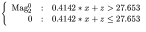
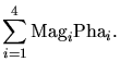
Fig. 5.3 shows the evolving front for this example. The view angle of this illustration is lower than for the Gaussian peaks in Fig. 5.2 and the front part of the resist cube is cut away in order to obtain a cross-section of the standing waves. The resist is etched backwards into the volume. The defect is located in the lower left quarter of the cube with the plane of reflection going from top left to bottom right. The vertical beam on the left hand side is directed towards the defect, building a V-like structure with the reflected beam. The thick vertical beam on the right passes the defect without being influenced. The outer shape of the evolving front is shaded in black, which facilitates the distinction between the outer and the inner side of the profile.

Figure 5.3: Reflective notching benchmark example.
\begin{figure}\psfrag{0.8 mu}[b][b][0.8]{0.8 $\mu$m}
\psfrag{0.8 um}[t][t][0.8]{...
...s[width=0.5\textwidth]{eps-dev/4-etch3dplot_00165.eps}}
\end{center}\end{figure}

The challenging part for this example is, that the maxima in the intensity should not exhibit any dependence on the positioning in the cellular structure and should evolve equally. As can be seen in Fig. 5.3 this dependence on the location within the simulation domain is clearly avoided by the cellular algorithm since all high intensity regions of the periodic standing waves evolve equally. This is true for the vertical beams in the same way as for the reflected beam, where the simulator forms the regular shape of the standing waves even for an arbitrary direction not perpendicular to any of the coordinate planes.

Moreover the simulator is able to develop the inclined tunnel underneath the resist surface. The cellular approach proves to be very robust in handling such cases and simultaneously allows a satisfactory resolution of the tunnel which conforms very closely to the expected cylindrical shape.

previous up next contents
Prev: 5.2.1 Multiple Gaussian Peaks Up: 5.2 Benchmarks Next: 5.2.3 Phase Shifted Outriggers


W. Pyka: Feature Scale Modeling for Etching and Deposition Processes in Semiconductor Manufacturing