

Chapter 1 Introduction
The manufacturing of semiconductor devices takes place in reactor chambers where the environment (pressure, temperature, chemicals) is strictly controlled, allowing precise fabrication of device-relevant structures in the nanometer range. The devices are fabricated starting from a plane wafer which typically is a thin slice of monocrystalline silicon. Ongoing advances of semiconductor device design have lead to complex three-dimensional (3D) designs and expensive manufacturing steps. This also manifests in shrinking admissible tolerances and increased development cost.
The high development costs and expensive experiments in the development cycle iterating between design and verification of new semiconductor devices are pushing the usage of predictive simulations for the manufacturing and operation of semiconductor devices. Those simulations, known as technology computer-aided design (TCAD) [1, 2] support the fabrication development by reducing the need for time-consuming and expensive experiments (costly materials and equipment). This accelerates the development cycle and reduces development costs.
TCAD simulations are divided into three categories: process TCAD, device TCAD, and circuit TCAD.
Process TCAD models the manufacturing processes of a semiconductor device by simulating processes which change the structure and/or topography (material layout) of the wafer, thus forming the individual devices [3]. The manufacturing processes include:
-
• etching (material is removed)
-
• deposition (material is added)
-
• oxidation (materials are oxidized, turning them into an oxide, which often have properties of insulators)
-
• ion implantation (dopants/impurities are implanted to change electrical material properties)
-
• annealing and diffusion (repairing crystal lattice defects and relocating dopants)
Device TCAD on the other hand uses the final generated structure to simulate the operation of a semiconductor device and calculate the electrical properties [4]. Circuit TCAD uses the device characteristics (electrical properties) provided by device TCAD to simulate the interaction of several devices, i.e., a simulation of an integrated circuit.
The context of this work is process TCAD simulation, which is further subdivided into two subcategories: Reactor scale and feature scale simulations.
Reactor vs. Feature Scale Simulations
Reactor scale simulations investigate the manufacturing process on a macroscopic scale, i.e., how chemicals (liquids or gases) enter the reactor chamber and how to ensure an equal distribution onto a wafer [5, 6]. Typically, all to-be-built devices on a wafer are processed simultaneously together, e.g., a wafer is exposed to oxygen at high temperatures, which results in oxidizing the surface. Reactor scale simulations are useful to model and analyze processing variations in different regions of the wafer. Minimizing those variations is essential to ensure a high device yield1. They are also used to predict variations between devices located on different wafers, in case several wafers are put into the reactor chamber at the same time, or in case processing several wafers subsequently before the reactor chamber is reset (extensively cleaned) to its initial condition.
Feature scale simulations, the focus of this work, describe the actual structural (potentially topographical) changes of the wafer. Feature scale simulations operate on the scale of a single device, or even on a sub-part of a device. The size of a device ranges from nanometers for logic devices to millimeters for power devices. Figure 1.1 shows a schematic of a typical simulation domain for a feature scale simulation, which represents a small part of a wafer with appropriate boundary conditions for the structure and other parameters, e.g., temperature or particle flux. The boundary conditions are potentially set by a previous reactor scale simulation.
The core of a feature scale simulation is the process model. The process model is the (simplified) physical description of the modeled manufacturing process. For example a process model for an etching process determines the etch rates for each material: The process model of a silicon oxidation process determines the rate at which silicon is transformed into silicon dioxide. Thus it is of utmost importance for feature scale simulations to have a high accuracy representation of the material regions (volumes or structure) of the device. Especially, the boundaries of material regions are important, because those are the areas which are directly affected by the process model, e.g., exposed silicon surfaces which directly interact with the available oxygen in the reactor chamber.

The following paragraphs introduce the numerical methods and algorithms2 used in the context of this thesis to track the topographical changes of these material regions.
1 Percentage of devices fulfilling the admissible tolerances in relation to all devices on a wafer.
2 An algorithm is a finite sequence of instructions used to solve a problem, i.e., complete a task.
Level-Set Method
The level-set method (cf. Chapter 4) tracks the material regions via the so-called level-set function [7]. The level-set function implicitly represents the boundary of a material region (interface between two materials regions, e.g., the outline of Material 1 and Material 2 in Figure 1.1) as the zero-level-set of the level-set function. By changing the zero-level-set of the level-set function the interface position is modified (material regions grow, shrink or deform). The implicit representation enables a robust handling of topological changes. The interface changes are prescribed by the process model which is typically defined via a partial differential equation (PDE), the level-set equation. The description of complex material regions using a level-set function is typically done on a discretized simulation domain. The considered rectilinear simulation domain is often discretized by a Cartesian grid, because it is convenient as derivatives used in process models as well as in the interface propagation can straight-forwardly be approximated by finite differences.
The level-set method is able to only track the boundary of material regions, which is computationally efficient compared to tracking the full volumes of material regions. In this case only a narrow-band of grid points adjacent to the interface is used for interface tracking, giving the name narrow-band level-set method [8]. Those grid points have to be stored efficiently, which is achieved using a sparse volume data representation, e.g., [9, 10]. Additionally, the level-set method allows straightforward extension of a simulation to higher dimensions, i.e., switching from two-dimensional (2D) to 3D simulations. The same algorithms are employed but need to process an additional coordinate. The application of the level-set method in process TCAD simulations is a well-established method for feature scale simulations, e.g., [11, 12, 13, 14, 15, 16, 17, 18, 19, 20, 21].
The above discussed benefits have led to a widespread use of the level-set method (spanning several research disciplines) for tracking moving interfaces. Application areas include computational fluid dynamics [22, 23, 24, 25, 26, 27, 28, 29, 30, 31], shape optimization [32, 33, 34, 35, 36, 37], computer graphics [38, 39, 40, 41, 42], image processing [43, 44, 45], and computational biophysics [46, 47, 48].
Explicit interface3 tracking approaches in the context of process TCAD simulations are described in [49, 50, 51]. Currently, explicit approaches are not further pursued, because of issues with respect to rarefaction or accumulation of polygons and with self-intersection of polygons representing the interface, which is especially a challenge for 3D simulations.
The discussion continues with a more detailed view on the discretization scheme used in this work.
3 The interface is represented as a set of polygons, segments or triangles, depending on the spatial dimensions.
Hierarchical Grids
The goal to achieve high accuracy in level-set process TCAD simulations forced the usage of fine spatial discretizations. However, fine spatial resolutions, especially for engineering-relevant 3D simulations, significantly increase the memory requirements and the run-time. On a Cartesian grid the run-time scales with the third power of the spatial discretization for a 3D simulation, easily and thus gets impractical.
A strategy to reduce the run-time is to employ high spatial resolutions only in some regions of the simulation domain. This strategy is known as adaptive mesh refinement (AMR). There are various approaches to AMR, where in this work the focus is on hierarchical grids. A hierarchical grid consists of several nested rectangular domains (blocks) each using a Cartesian discretization with varying spatial resolutions. Their possible placement in also indicated in Figure 1.1. The details of the used hierarchical grid are presented in Chapter 2. The approach using hierarchical grids based on Cartesian grids is convenient, because the same numerical schemes to approximate derivatives as on a Cartesian grid can be employed.
Time Stepping
The time evolution of the material regions is typically described by a PDE. Typically, the PDE is discretized in time and advanced in time steps until the final simulation time is reached. Combined with the spatial discretization using hierarchical grids the computational steps4 of the level-set method in every time step are:
-
• Interface Velocity: Coupling the process (physical accurate) model, describing the deformation of the interface, to the level-set representation of the material regions.
-
• Velocity Extension: Extending a velocity field from an interface (i.e., surface of a material region) to the entire computational domain. In particular, velocity refers to the physically determined velocity prescribing the movement of the interface.
-
• Advection: Using the previously extended velocity field to solve the advection equation of the interface, actually changing the interface position.
-
• Re-Distancing: Re-normalizing the signed-distance field to an interface. This step is essential for a robust interface representation and a geometric interpretation of the level-set function away from the interface.
-
• Re-Gridding: Adapting the hierarchical grid structure to fit the blocks of a fine spatial resolution to the deformed and displaced interfaces describing the material regions.
The computational steps (and algorithms used to solve the computational steps) of the level-set method are presented and discussed further in Chapter 4.
In addition to AMR this work also uses parallelization approaches to accelerate some key algorithms for process TCAD simulations. Therefore, the following section provides a motivation regarding the importance of parallelization.
4 A computational step is a task for which one ore more algorithms may be employed, e.g., Sorting is a computational step: Any sorting algorithm is a valid choice to complete the task.
Parallelization
While early research on parallel computations dates back to the 1960s, starting in the early 2000s the number of cores on a central processing unit (CPU) increased as the frequency wall was hit5, limiting the exponential growth of serial performance (cf. Figure 1.2). This trend continues until today where top CPUs can offer over 100 logical cores, e.g., an AMD Ryzen Threadripper 3990X offers 128 logical cores [52], or an Intel Xeon Platinum 9282 has 112 logical cores [53]. Thus, to utilize the gain in available computing power the developed algorithms must be parallel: This work focuses on shared-memory parallel approaches to utilize the high degree of parallelism provided by the discussed high core counts of modern CPUs. Computer programs6 implementing parallel algorithms on shared-memory systems use threads7 to distribute their computations among the available CPU cores.

Hierarchical grids provide an inherent potential for parallelism: Parallelization of algorithms on hierarchical grids is often implemented so that on each block the algorithm is performed independently in parallel. Obviously, this requires a synchronization step to align the parallel calculated results. However, this approach delivers only good parallel efficiency, if multiple blocks per thread are available, allowing for load-balancing to counter imbalances imposed by strongly varying block sizes and numbers. Load imbalances happen, if some threads have completed their task (share of computations), but have to wait for other threads to finish their task before they may proceed with their next task (synchronization barrier).
A concrete feature scale simulation example is presented in the next section to show the capability of current process TCAD simulations and to establish a baseline for the computational performance via benchmarking the simulation.
5 The frequency of CPUs could not be reliably increased further, due to power and heat limitations.
6 A computer program is a set of instructions describing a specific implementation of an algorithm to a computer.
7 A thread is the smallest set of instructions managed and independently scheduled by the operating system for execution on a CPU core. Each thread has access to the entire system memory.
1.1 Motivational Example: Thermal Oxidation
Thermal oxidation is a fundamental processing step in the manufacturing of semiconductor devices [54]. It is used to create an insulating or protective layer of silicon dioxide \(\left (\text {SiO}_2\right )\), by exposing a silicon \(\left (\text {Si}\right )\) surface to oxygen gas \(\left (\text {O}_2\right )\) or water vapor \(\left (\text {H}_2\text {O}\right )\) at temperature ranges from 800 °C to 1400 °C in an oxidation reactor chamber (furnace). The oxidation furnace is usually operated using heating coils in combination with a temperature measurement and control system. Thermal oxidation is also used to grow gate oxides insulating the gate from the source and drain of metal-oxide semiconductor field effect transistors (MOSFETs), which are among the basic building blocks for microelectronic circuits in the semiconductor industry.
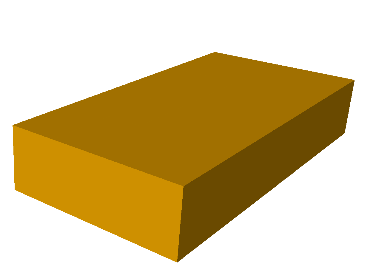
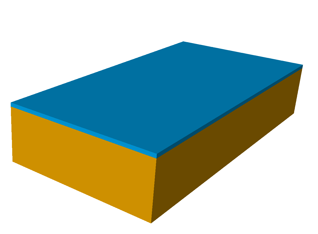
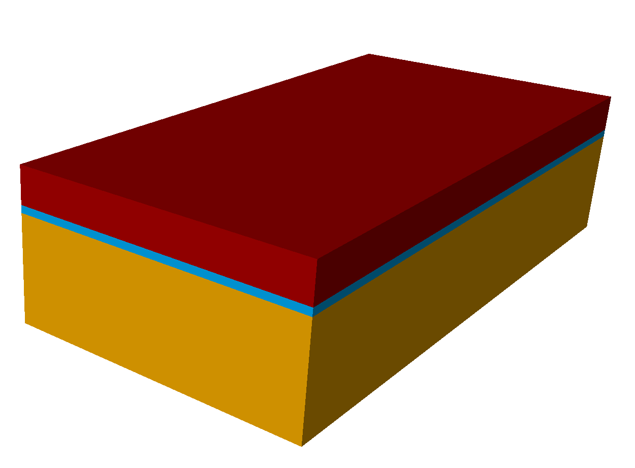
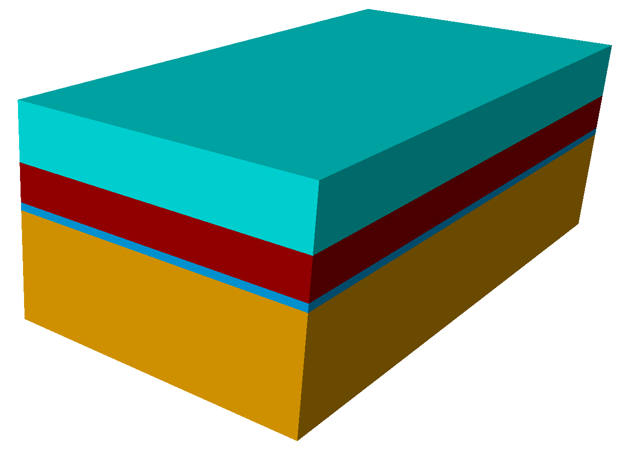
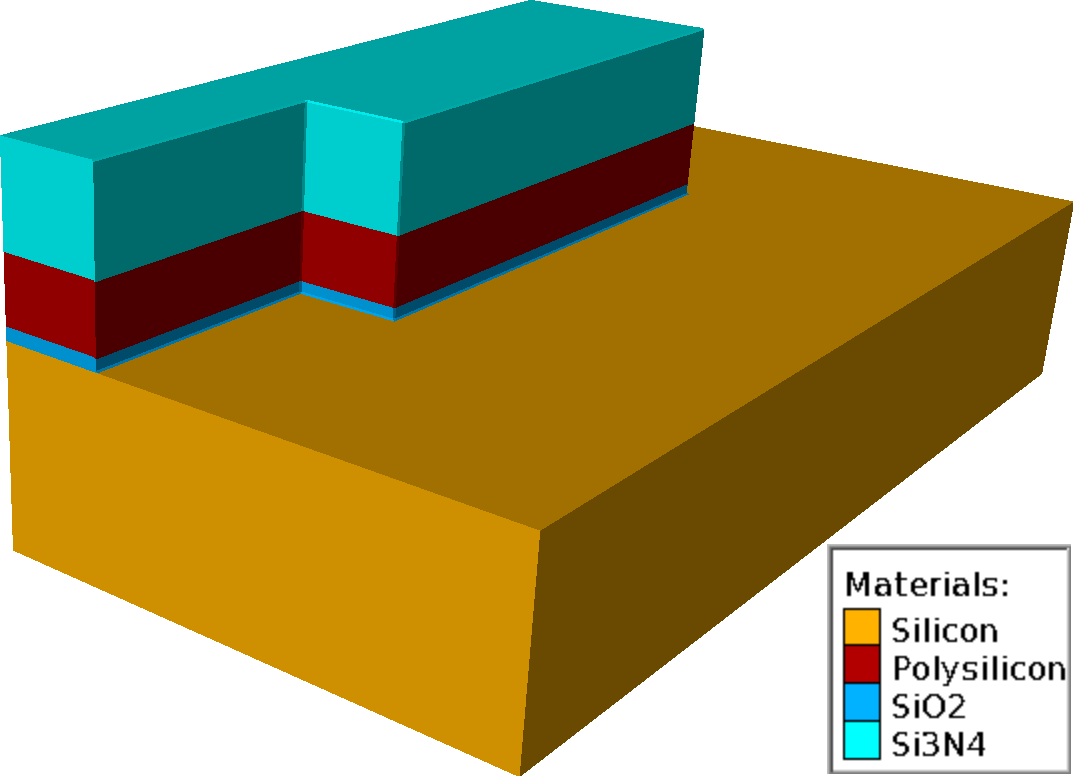
For the thermal oxidation process a rectilinear simulation domain with symmetric (reflective) boundary conditions is considered. Figure 1.3 shows all process steps of a thermal oxidation simulation example. The initial material layout of the thermal oxidation simulation example is created using constructive solid geometry (CSG) operations. On the bulk silicon (cf. Figure 1.3a) several materials are deposited (in layers covering the whole simulation domain) (cf. Figure 1.3b – Figure 1.3d) and then parts of the deposited materials are geometrically etched (one could consider this as a very rudimentary process model based on simplified physics) using an L-shaped mask (cf. Figure 1.3e). In particular, the deposited material layers from bottom to top (in order of deposition) are silicon dioxide8 \(\left (\text {SiO}_2\right )\), polysilicon (Polysilicon), and silicon nitride \(\left (\text {Si}_3\text {N}_4\right )\). This represents the starting point of the physically accurate simulated thermal oxidation process. Figure 1.3e and Figure 1.3f show the material regions before and after the 15 min thermal oxidation process at 1000 °C. The silicon and polysilicon material regions shrink, because they are turned into oxide. The process expands the created oxide compared to the previously present material (silicon and polysilicon) and deforms the silicon nitride on top9.

The investigation continues on the level-set method specifics of the example thermal oxidation simulation such as the material representation and the structure of hierarchical grids.
8 In semiconductor manufacturing this is often called just oxide, because silicon is the predominantly oxidized material.
9 The characteristic emergence of features resembling a bird’s beak [51, 55] is observed between the silicon dioxide and the polysilicon.
Level-Set Method on Hierarchical Grids
Figure 1.4 shows the interfaces represented by the four level-set functions (one for each material) used for the initial material layout of the thermal oxidation simulation shown in Figure 1.3e. The interfaces do not enclose a material region directly, but are selected so that they avoid material region overlaps and enable best computational performance. The level-set used to represent the silicon nitride material region is identical to the surface of the structure (surface visible form the outside). This is beneficial to the simulation, because the surface of the structure is the area of exchange of the structure with the reactants from the reactor chamber. Additionally, Figure 1.4 also shows the layout (placement and size) of the blocks used on the hierarchical grid. Those blocks (rectangular domains) are shown by their outline colored in black. The outermost block covers the full simulation domain with a low spatial resolution, its boundaries are identical to the boundaries of the simulation domain. The remaining blocks which employ a higher spatial resolution are located around corners and edges of material regions (interfaces).
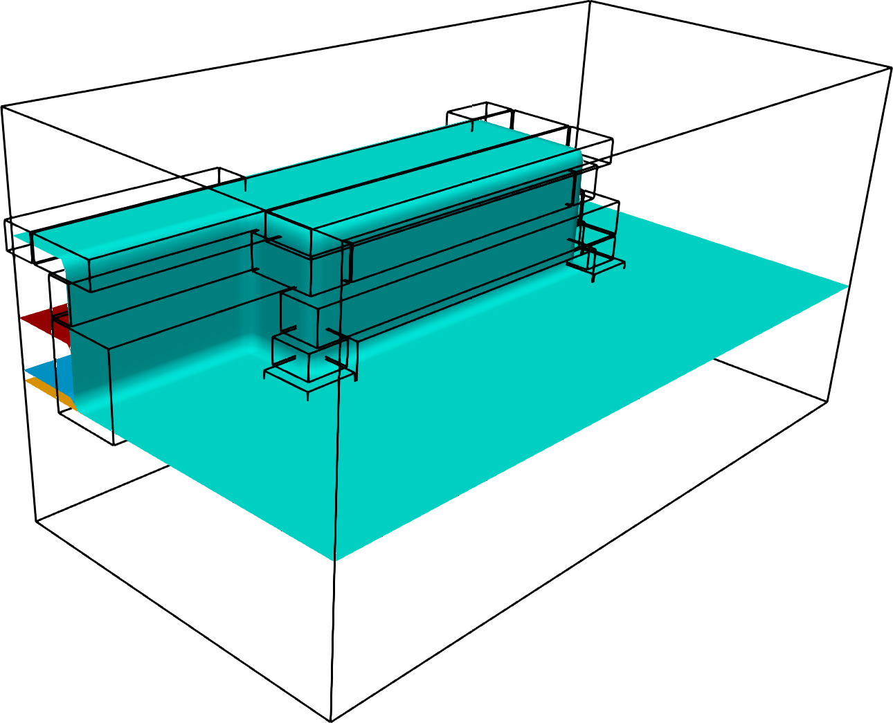
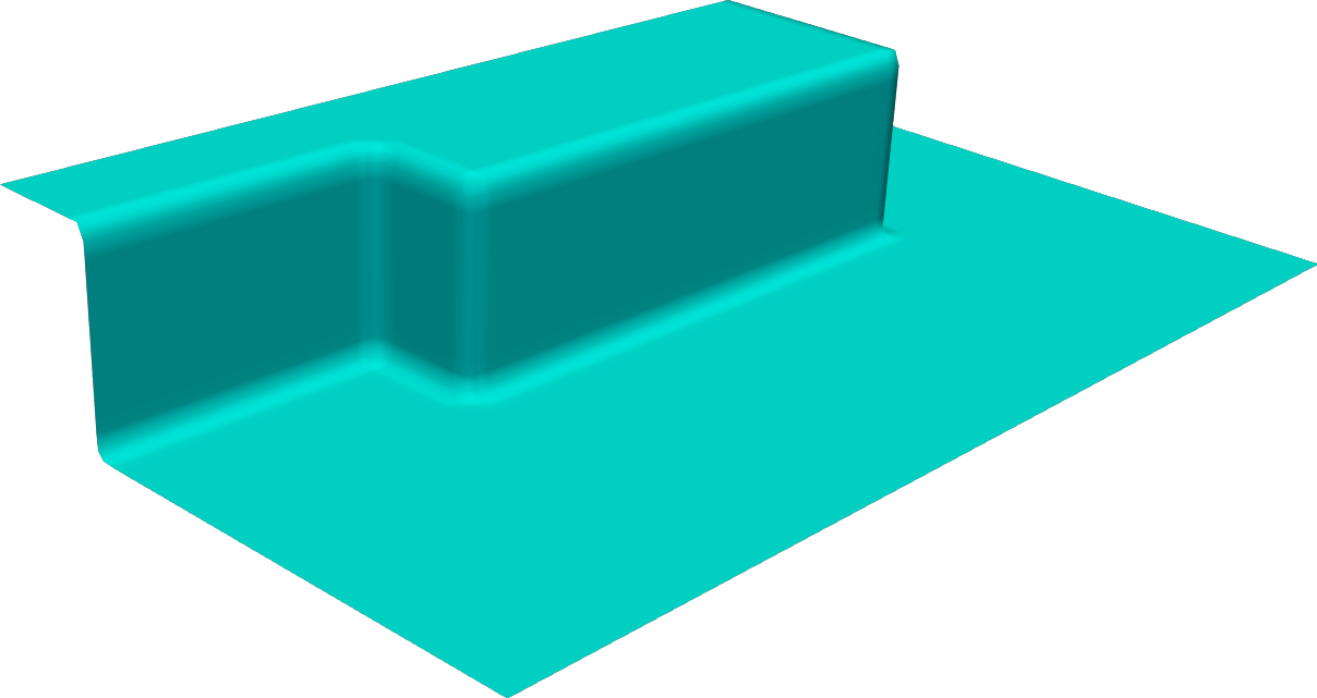
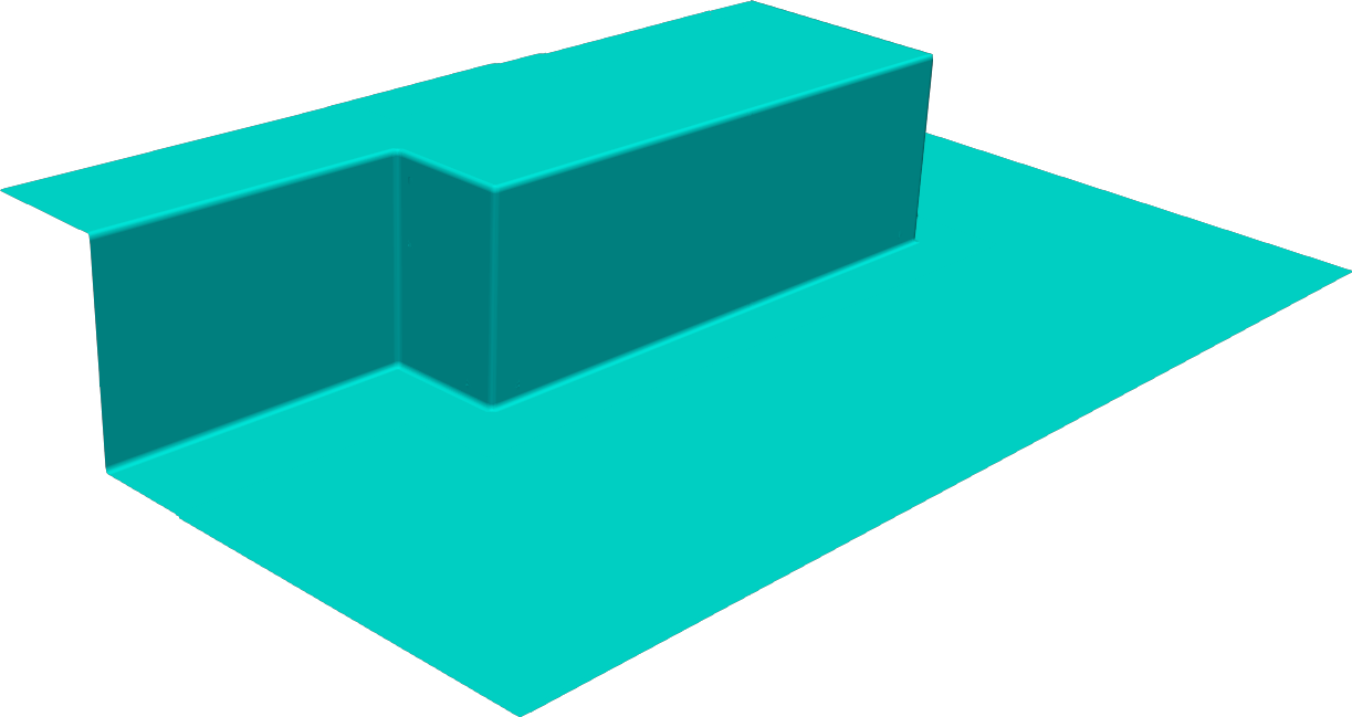
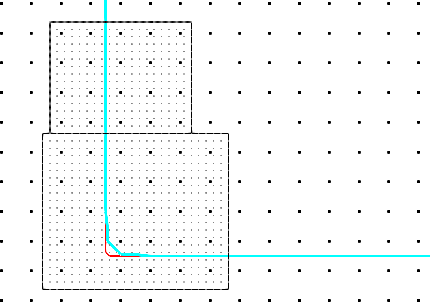
Figure 1.5 shows the zero-level-set of the level-set function used for representing the silicon nitride for a low (coarse) spatial resolution and a four times increased (finer) spatial resolution. The difference between those two spatial resolutions is striking at the edges and corners. The level-set inherent rounding of analytic sharp corners is directly related to the spatial resolution, affecting one to two grid points around the corner. Thus if only those corners are resolved by a grid with a higher finer spatial resolution the same accuracy for the interface is achieved, favoring an approach based on hierarchical grids (cf. Figure 1.6).
In the thermal oxidation example comparing the approach based on hierarchical grids (using \(664\,704\) grid points) to a reference discretization using a single Cartesian grid with an uniform high spatial resolution (using \(8\,192\,000\) grid points) shows that the number of grid points is reduced by a factor of 12.
A key aspect of a hierarchical grid is to utilize the gained accuracy on the finer spatially resolved regions also on the coarse grid. Typically, this is done via an interpolation of the grid points of the coarse grid. The gained accuracy is especially beneficial for features for which the coarse grid is not able to resolve them correctly. Such features are in particular corners (cf. Figure 1.6) and thin trenches. The problem is that a straightforward interpolation does not affect grid points which are not covered by finer spatial resolutions. The coupling of the grids (the interpolation) is mainly performed in the Re-Distancing step, therefore, an improvement in this computational step has the greatest impact on the overall accuracy (cf. Section 4.2.6).
Benchmark Baseline
To analyze where the computational bottlenecks of the level-set method are, the thermal oxidation process is benchmarked using a reference simulator: Victory Process (cf. Section 4.3). The compute system used for the benchmark is a representative industrial compute server (ICS) (cf. Section 3.2).
The measured run-times for the computational steps of the level-set method (ordered chronologically) are shown in Figure 1.7 for every time step of the simulation separately. There are a total of 27 time steps involved in the considered oxidation simulation. The run-time for each time step increases during the simulation, because the regions where a high spatial discretization is required to sustain an accurate simulation increase in size, thus more grid points are present which in turn require more computations.

Each of the computational steps contributes to the total run-time. The three computational steps, which are the main contributors to the total run-time, are:
-
1. Advection (35.9 %),
-
2. Re-Distancing (30.7 %), and
-
3. Velocity Extension (22.1 %).
The biggest contributor – the Advection – is out of scope of the conducted research, because it has already been extensively studied [57, 58, 59]. Typical employed parallel algorithms allow for independent computations for each grid point enabling a straightforward parallelization.
This thesis, however, focuses on the computational steps Velocity Extension and Re-Distancing, because as can clearly be seen they are key contributors to the overall simulation run-time. Together they are responsible for more than half of the serial run-time, demanding efficient parallelization approaches to mitigate the serious performance hit.
The task for both computational steps is similar: Each has to extend a given field (either a velocity field or a signed-distance field) from the interface to the computational domain. However, the difference is whether the to-be-extended field influences the control flow of the extension, i.e., the order in which the values for the grid points are computed. In case of Velocity Extension the to-be-extended field (the interface velocity) does not influence the control flow, i.e., for different velocity fields at the interface, the order of the computations stays the same (the extended velocity values are obviously different). However, in case of Re-Distancing the to-be-extended field (the signed-distance10) does influence the control flow. The algorithmic solution for both computational steps is based on the fast marching method (FMM) [60].
The FMM finds wide spread use and parallel solution approaches are available (in cases where the control flow is influenced by the field) [61]. These approaches typically consider only Cartesian grids. A parallel algorithm considering hierarchical grids was developed albeit offering limited scalability due to load-balancing issues rooted in a non-optimal dependency on the number and dimension variations of hierarchical grid blocks [62]. For example using 10 threads for the previously shown thermal oxidation example leads to load-imbalances, because the hierarchical grid consists (depending on the time step) of 17 blocks only: In this case, three threads would only process a single block, preventing the compensation of varying run-times between blocks.
Hierarchical grids require data exchange between levels of different spatial resolution. Especially, for Re-Distancing high accuracy schemes are desired to fully utilize the advantages of hierarchical grids.
For the Velocity Extension the same algorithm (the FMM) can theoretically be applied. The nature of an unchanged control flow of computations for the FMM should allow for higher optimizations of the computations. The dependencies of the computations could be determined beforehand, enabling shorter run-times and yielding opportunities for advanced parallelization.
1.2 Research Goals
The main goal of the conducted research is to reduce the turnaround time of 3D feature scale process TCAD simulations using the level-set method on hierarchical grids. The focus is to accelerate two of the key computational steps of the level-set method: 1) Velocity Extension and 2) Re-Distancing. These computational steps are selected because they significantly contribute to the overall run-time as previously discussed (cf. Figure 1.7).
The acceleration should be achieved by first parallelizing the Velocity Extension on a single Cartesian grid exploiting the computation order and then tailoring the developed parallel algorithm to hierarchical grids.
For the Re-Distancing an advanced block decomposition has to be developed for the FMM, which in principle allows for efficient parallelization on hierarchical grids by putting emphasis on load-balancing.
A further important goal is to increase the numerical accuracy of Re-Distancing for hierarchical grids, especially in cases where only the higher grid resolutions enable the representation of a feature like a thin trench. The computational overhead shall be minimized.
Research Setting
The research presented in this work was conducted within the scope of the Christian Doppler Laboratory for High Performance TCAD. The Christian Doppler Association funds cooperations between companies and research institutions pursuing application-orientated basic research. In this case, the research was lead by Josef Weinbub and involved the Institute for Microelectronics at the TU Wien and Silvaco Inc., a company developing and providing electronic device automation and TCAD software tools.
1.3 Outline
Chapter 2 presents an overview of spatial discretization methods, adaptive mesh refinement, and the implementation of the hierarchical grid used in the reference simulation software.
Chapter 3 presents an overview of the terms used in parallelization and gives context with respect to the compute systems used for evaluating the performance of the algorithmic developments.
Chapter 4 portrays the level-set method with a special focus on process TCAD simulations. The mathematical background for the level-set method is given and all computational steps are discussed which have already been shown in Figure 1.7. The numerical implementation of the computational steps in the reference simulator, i.e., the reference simulation workflow, is discussed. Available simulation software for process TCAD simulations is listed.
Chapter 5 presents the newly developed parallelized velocity extension algorithm, which is first introduced for operating on a single Cartesian grid. Subsequently, an extension tailored towards the use on hierarchical grids is presented. The FMM, because it is the foundation of the improved computational steps, is presented. The parallelized velocity extension algorithm is analyzed and evaluated based on two representative process TCAD simulation examples for scalar and vector velocity fields, discussing run-time performance metrics.
Chapter 6 proposes an advanced parallelization algorithm for the FMM used in the Re-Distancing step. The key contribution is a novel domain decomposition approach to enable better load-balancing during the execution of the FMM, resulting in a shorter run-time for high core count CPUs. The granularity of the decomposition and the frequency of synchronizations is particularly focused on in the analysis. The parallel performance is evaluated based on representative interfaces (level-set functions) taken from typical process TCAD simulations.
Chapter 7 presents an algorithm to increase the accuracy of the signed-distance field on coarser levels of the hierarchical grid, by using a bottom-up correction algorithm. The algorithm is evaluated on generic test cases resembling geometries occurring in process TCAD simulations. This enables to compute the exact solution as a reference solution and, therefore, an accurate comparison of the corrected signed-distance field to the exact solution is possible.
In the last chapter, Chapter 8 the key findings of this thesis are summarized, the motivational example is revisited, and new ideas are proposed for future research.