Subsections

4.1.8 Boundary Conditions

For the solution of the semiconductor equations a closed domain is required. Boundary conditions for the unknowns in a certain segment must be specified at the boundaries of that segment. Depending on the number of segments (one or two) and the type of the quantity of the unknown (distributed or non-distributed) several model types can be separated [267]. However, in order to illustrate the basic boundary conditions such a differentiation is not needed and therefore not provided here.

4.1.8.1 Artificial Boundaries

The simulation domain usually includes only a single device. In order to separate it from the neighboring devices artificial boundaries, which have no physical origin, are introduced. Through the Neumann boundary conditions a self-contained domain is guaranteed. The fluxes across the boundary are set to zero:

$\displaystyle \ensuremath{\mathitbf{n}}\cdot\ensuremath{\mathitbf{E}}=0,   \e...
...suremath{\mathitbf{n}}\cdot\ensuremath{\mathitbf{S}}_\ensuremath{\mathrm{L}}=0.$ (4.28)

$ \ensuremath{\mathitbf{n}}$ is an outward-orientated vector normal to the boundary. (4.28) define the boundary conditions for a semiconductor segment, while for an insulator the first two conditions are sufficient.

4.1.8.2 Semiconductor/Metal

Ohmic Contact:

Ohmic contacts are defined by Dirichlet boundary conditions: the contact potential $ \psi_\ensuremath{\mathrm{s}}$, the carrier contact concentration $ n_\ensuremath{\mathrm{s}}$ and $ p_\ensuremath{\mathrm{s}}$, and in the case of a HD simulation the carrier contact temperatures $ \ensuremath{T_\ensuremath{n}}$ and $ \ensuremath{T_\ensuremath{p}}$ are fixed. The metal quasi-Fermi level (which is specified by the contact potential $ \psi_\ensuremath{\mathrm{m}}$) is equal to the semiconductor quasi-Fermi level. The model assumes charge-neutrality on the boundary. The contact potential at the semiconductor boundary is:

$\displaystyle \psi_\ensuremath{\mathrm{s}}=\psi_\ensuremath{\mathrm{m}}+\varphi_\ensuremath{\mathrm{bi}},$ (4.29)

where $ \varphi_\ensuremath{\mathrm{bi}}$ is the built-in potential:
$\displaystyle \varphi_\ensuremath{\mathrm{bi}}$ $\displaystyle =$ $\displaystyle \frac{\ensuremath{\mathrm{k}}_\ensuremath{\mathrm{B}}\ensuremath{...
...net}}}+ \sqrt{\ensuremath{C_\ensuremath{\mathrm{net}}}^2+4C_1C_2}\right)\right)$ (4.30)
  $\displaystyle =$ $\displaystyle -\frac{\ensuremath{\mathrm{k}}_\ensuremath{\mathrm{B}}\ensuremath...
...net}}}+\sqrt{\ensuremath{C_\ensuremath{\mathrm{net}}}^2+4C_1C_2}\right)\right).$ (4.31)

$ \ensuremath{C_\ensuremath{\mathrm{net}}}$ is the net concentration of dopants and other charged defects at the contact boundary. The variables $ C_1$ and $ C_2$ are defined by [268]
$\displaystyle C_1$ $\displaystyle =$ $\displaystyle \ensuremath{N_\mathrm{C}} \ensuremath{\mathrm{exp}}\left(\frac{-...
...suremath{\mathrm{k}}_\ensuremath{\mathrm{B}}\ensuremath{T_{\mathrm{L}}}}\right)$ (4.32)
$\displaystyle C_2$ $\displaystyle =$ $\displaystyle \ensuremath{N_\mathrm{V}} \ensuremath{\mathrm{exp}}\left(\frac{-...
...suremath{\mathrm{k}}_\ensuremath{\mathrm{B}}\ensuremath{T_{\mathrm{L}}}}\right)$ (4.33)

where $ \ensuremath{N_\mathrm{C}}$ and $ \ensuremath{N_\mathrm{V}}$ are the effective density of states.

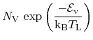
The carrier concentrations in the semiconductor are pinned to the equilibrium carrier concentrations at the contact:

$\displaystyle n_S$ $\displaystyle =$ $\displaystyle \ensuremath{N_\mathrm{C}} \ensuremath{\mathrm{exp}}\left(\frac{-...
...suremath{\mathrm{k}}_\ensuremath{\mathrm{B}}\ensuremath{T_{\mathrm{L}}}}\right)$ (4.34)
$\displaystyle p_S$ $\displaystyle =$ $\displaystyle \ensuremath{N_\mathrm{V}} \ensuremath{\mathrm{exp}}\left(\frac{\...
...suremath{\mathrm{k}}_\ensuremath{\mathrm{B}}\ensuremath{T_{\mathrm{L}}}}\right)$ (4.35)

This model works properly, only if a high doping ( $ \ge
10^{18}$cm$ ^{-3}$) in the semiconductor is guaranteed.

The carrier temperatures $ \ensuremath{T_\ensuremath{n}}$ and $ \ensuremath{T_\ensuremath{p}}$ are set equal to the lattice temperature $ \ensuremath{T_{\mathrm{L}}}$:

$\displaystyle \ensuremath{T_\ensuremath{n}}=\ensuremath{T_{\mathrm{L}}},    \ensuremath{T_\ensuremath{p}}=\ensuremath{T_{\mathrm{L}}}.$ (4.36)

Thermal Interface:

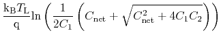
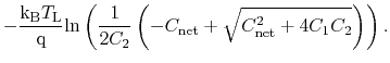
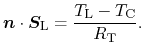
If a contact temperature $ \ensuremath{T_\ensuremath{\mathrm{C}}}$ is specified, the lattice temperature is calculated using $ \ensuremath{T_\ensuremath{\mathrm{C}}}$ and a thermal resistance $ R_\ensuremath{\mathrm{T}}$. The thermal heat flow density $ \ensuremath{\mathitbf{S}}_\ensuremath{\mathrm{L}}$ at the contact boundary reads:

$\displaystyle \ensuremath{\mathitbf{n}}\cdot\ensuremath{\mathitbf{S}}_\ensurema...
...mathrm{L}}}-\ensuremath{T_\ensuremath{\mathrm{C}}}}{R_\ensuremath{\mathrm{T}}}.$ (4.37)

If no thermal resistance is specified, an isothermal boundary condition is assumed and the lattice temperature $ \ensuremath{T_{\mathrm{L}}}$ is set equal to the contact temperature:

$\displaystyle \ensuremath{T_{\mathrm{L}}}=\ensuremath{T_\ensuremath{\mathrm{C}}}.$ (4.38)

In case of a DD simulation with self-heating an additional thermal energy is accounted for. It is generated, when the carriers transcend the potential difference between the conduction or valence band and the metal quasi-Fermi level. The energy equation reads:

$\displaystyle \ensuremath{\mathitbf{J}}_n \left( \frac{\ensuremath{\ensuremath{...
...{\nabla}}}\ensuremath{\cdot}}\ensuremath{\mathitbf{S}}_\ensuremath{\mathrm{L}}.$ (4.39)

The expression $ \ensuremath{\ensuremath{\ensuremath{\mathitbf{\nabla}}}\ensuremath{\cdot}}\ensuremath{\mathitbf{S}}_\ensuremath{\mathrm{L}}$ denotes the surface divergence of the thermal heat flux at the boundary considered. In case of a HD simulation with self-heating the thermal heat flow across the boundary is accounted for self-consistently.

Metal Resistance:

It is possible to include an electric line resistance of the contact $ R_\ensuremath{\mathrm{C}}$ using:

$\displaystyle \psi_m=V_\ensuremath{\mathrm{C}}-I_\ensuremath{\mathrm{C}}R_\ensuremath{\mathrm{C}}$ (4.40)

with $ V_\ensuremath{\mathrm{C}}$ the applied terminal voltage and $ I_\ensuremath{\mathrm{C}}$ the current through the contact.

Schottky Contact:

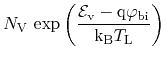
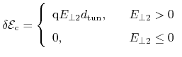
At the Schottky contact mixed boundary conditions apply. The contact potential $ \psi_\ensuremath{\mathrm{s}}$, the carrier contact concentration $ n_\ensuremath{\mathrm{s}}$ and $ p_\ensuremath{\mathrm{s}}$, and in the case of a HD simulation, the contact carrier temperatures $ \ensuremath{T_\ensuremath{n}}$ and $ \ensuremath{T_\ensuremath{p}}$ are fixed. The semiconductor contact potential is the difference between the metal quasi-Fermi level and the metal work function difference $ \psi_\ensuremath{\mathrm{w}}$:

$\displaystyle \psi_\ensuremath{\mathrm{s}}=\psi_\ensuremath{\mathrm{m}}-\psi_\ensuremath{\mathrm{w}}$ (4.41)

where

$\displaystyle \psi_\ensuremath{\mathrm{w}}=-\frac{\ensuremath{\ensuremath{\mathcal{E}}_{\ensuremath{\mathrm{w}}}}}{\mathrm{q}}.$ (4.42)

The difference between the conduction band energy $ \ensuremath{\ensuremath{\mathcal{E}}_{\ensuremath{\mathrm{c}}}}$ and the metal work function energy gives the work function difference energy $ \ensuremath{\ensuremath{\mathcal{E}}_{\ensuremath{\mathrm{w}}}}$, which is the so called barrier height of the Schottky contact, also denoted as $ \ensuremath{\phi_\ensuremath{\mathrm{B}}}$. The applied boundary conditions are:
$\displaystyle \ensuremath{\mathitbf{n}}\cdot\ensuremath{\mathitbf{J}}_\ensuremath{\mathrm{n}}$ $\displaystyle =$ $\displaystyle -\mathrm{q}\upsilon_\ensuremath{\mathrm{n}} (n_0-n_\ensuremath{\mathrm{s}})$ (4.43)
$\displaystyle \ensuremath{\mathitbf{n}}\cdot\ensuremath{\mathitbf{J}}_\ensuremath{\mathrm{p}}$ $\displaystyle =$ $\displaystyle \mathrm{q}\upsilon_\ensuremath{\mathrm{p}} (p_0-p_\ensuremath{\mathrm{s}}),$ (4.44)

where $ \upsilon_\ensuremath{\mathrm{n}}$ and $ \upsilon_\ensuremath{\mathrm{p}}$ are the recombination velocities. The carrier concentrations read:
$\displaystyle n_\ensuremath{\mathrm{s}}=\ensuremath{N_\mathrm{C}} \ensuremath{...
...suremath{\mathrm{k}}_\ensuremath{\mathrm{B}}\ensuremath{T_{\mathrm{L}}}}\right)$     (4.45)
$\displaystyle p_\ensuremath{\mathrm{s}}=\ensuremath{N_\mathrm{V}} \ensuremath{...
...uremath{\mathrm{k}}_\ensuremath{\mathrm{B}}\ensuremath{T_{\mathrm{L}}}}\right),$     (4.46)

where $ \ensuremath{\ensuremath{\mathcal{E}}_{\ensuremath{\mathrm{f}}}}$ is the Fermi level in the semiconductor. If the values of $ \upsilon_\ensuremath{\mathrm{n}}$ and $ \upsilon_\ensuremath{\mathrm{p}}$ are set to zero, the current through the Schottky contact is suppressed. The Schottky contact boundary conditions for the carrier temperatures $ \ensuremath{T_\ensuremath{n}}$ and $ \ensuremath{T_\ensuremath{p}}$ and for the lattice temperature are similar to those which apply for the Ohmic contact: (4.36) and (4.37) or (4.38).

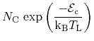
For the equilibrium situation, the quasi-equilibrium concentrations $ n_0$ and $ p_0$ can be rewritten:

$\displaystyle n_0$ $\displaystyle =$ $\displaystyle \ensuremath{N_\mathrm{C}} \ensuremath{\mathrm{exp}}\left(\frac{-...
...suremath{\mathrm{k}}_\ensuremath{\mathrm{B}}\ensuremath{T_{\mathrm{L}}}}\right)$ (4.47)
$\displaystyle p_0$ $\displaystyle =$ $\displaystyle \ensuremath{N_\mathrm{V}} \ensuremath{\mathrm{exp}}\left(\frac{-...
...uremath{\mathrm{k}}_\ensuremath{\mathrm{B}}\ensuremath{T_{\mathrm{L}}}}\right).$ (4.48)

The recombination velocities are calculated from:

$\displaystyle \upsilon_\ensuremath{\mathrm{n}}=A^{*}\frac{\ensuremath{T_{\mathrm{L}}}^2}{\mathrm{q}\ensuremath{N_\mathrm{C}}}$ (4.49)

where $ A^{*}$ is the Richardson constant.

Typical values for the Schottky barrier heights of common semiconductor barriers are listed in Table 4.1. Values measured by different methods (I-V and C-V) for n-GaN/metal differ significantly. This is caused by defects in the surface region, which enhance the tunneling effect and therefore have an impact on the Richardson constant [269,270]. The exact value of the barrier height depends also on orientation, stress, and polarity of the GaN layer [271]. No data is provided for contacts on InN as most metals show ohmic behavior [272]. Schottky barrier height varies with annealing temperature: generally it is reduced after annealing.


Table 4.1: Schottky barrier heights of common contacts.
Materials $ \ensuremath{\phi_\ensuremath{\mathrm{B}}}$[eV] Ref. Materials $ \ensuremath{\phi_\ensuremath{\mathrm{B}}}$[eV] Ref.
n-GaN/Au 0.87-1.1 [273,274] In$ _{x}$Al$ _{x}$N/Pd 1.56 [275]
n-GaN/Ni 0.95-1.13 [273] In $ _\ensuremath{\mathrm{0.17}}$Al $ _\ensuremath{\mathrm{0.83}}$N/Ni 0.75 [276]
p-GaN/Ni 2.68-2.87 [277] p-In $ _\ensuremath{\mathrm{0.15}}$Ga $ _\ensuremath{\mathrm{0.85}}$N/Ni 0.39 [278]
Al $ _\ensuremath{\mathrm{0.11}}$Ga $ _\ensuremath{\mathrm{0.89}}$N/Ni 0.94-1.24 [279] In $ _\ensuremath{\mathrm{0.1}}$Ga $ _\ensuremath{\mathrm{0.9}}$N/Pt 0.62 [270]
Al $ _\ensuremath{\mathrm{0.15}}$Ga $ _\ensuremath{\mathrm{0.85}}$N/Ni 1.26 [280] In $ _\ensuremath{\mathrm{0.1}}$Ga $ _\ensuremath{\mathrm{0.9}}$N/Ni 1.39 [270]
Al $ _\ensuremath{\mathrm{0.23}}$Ga $ _\ensuremath{\mathrm{0.77}}$N/Ni 1.02-1.30 [279] Al $ _\ensuremath{\mathrm{0.07}}$In $ _\ensuremath{\mathrm{0.02}}$GaN/Ni 0.98-0.93 [281]

4.1.8.3 Insulator/Metal

A model similar to the Schottky contact model is used to calculate the insulator contact potential. The semiconductor contact potential is the difference of the metal quasi-Fermi level and the metal work function difference potential similar to (4.41) and (4.42). The lattice temperature is set equal to the contact temperature (4.38).

4.1.8.4 Semiconductor/Insulator

In the absence of surface charges the normal component of the dielectric displacement and the potential are continuous:

$\displaystyle \ensuremath{\mathitbf{n}}\cdot\varepsilon_\ensuremath{\mathrm{s}}...
...hrm{ins}}=0,    \psi_\ensuremath{\mathrm{s}}=\psi_\ensuremath{\mathrm{ins}}.$ (4.50)

In the presence of surface charges along the interface, the dielectric displacement obeys the law of Gauß:

$\displaystyle \ensuremath{\mathitbf{n}}\cdot\varepsilon_\ensuremath{\mathrm{s}}...
...uremath{\mathitbf{E}}_\ensuremath{\mathrm{ins}}=\sigma_\ensuremath{\mathrm{s}},$ (4.51)

where $ \sigma_\ensuremath{\mathrm{s}}$ is the interface charge density. This distributed surface charge is introduced to describe the Fermi level pining at the surface due to a high trap density of states.

At the semiconductor/insulator interface the current densities and heat fluxes normal to the interface vanish.

$\displaystyle \ensuremath{\mathitbf{n}}\cdot\ensuremath{\mathitbf{J}}_\ensurema...
...uremath{\mathitbf{n}}\cdot\ensuremath{\mathitbf{S}}_\ensuremath{\mathrm{n,p}}=0$ (4.52)

The lattice temperature at the interface is continuous.

4.1.8.5 Semiconductor/Semiconductor

The calculation of the electrostatic potential at the interfaces between two semiconductor segments is similar to that for semiconductor/insulator interfaces:

$\displaystyle \ensuremath{\mathitbf{n}}\cdot\varepsilon_\ensuremath{\mathrm{s1}...
...{\mathrm{s}},    \psi_\ensuremath{\mathrm{s1}}=\psi_\ensuremath{\mathrm{s2}}$ (4.53)

The interface charge can take any value including zero. The way to calculate the exact value depending on the materials is discussed in Section 4.5. The subscripts are used to distinguish between the two semiconductor segments on both sides of of the interface.

To calculate the carrier concentrations and the carrier temperatures at the interface, three different approaches are considered:

Each model can be specified for electrons and holes for each semiconductor/semiconductor interface.

In the following $ J_\ensuremath{\mathrm{n}}$ denotes the normal to the interface component of the current density $ \ensuremath{\mathitbf{J}}$, $ S_\ensuremath{\mathrm{n}}$ the energy flux density component, and $ \Delta E_\nu$ the difference in the conduction band edges $ \Delta\ensuremath{\ensuremath{\mathcal{E}}_{\ensuremath{\mathrm{c}}}}$. The effective electron mass is denoted by $ m_{i}$. The subscripts denote the semiconductor segment $ i$. Only the equations for electrons are given, those for holes can be deduced accordingly.

Continuous Quasi-Fermi Level Model:

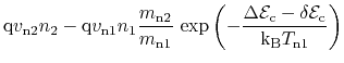
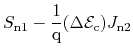
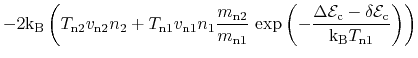
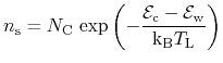
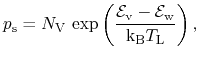
Dirichlet boundary conditions are applied, when the CQFL is used. The carrier concentrations are determined so that the quasi-Fermi levels remains continuous across the interface [134].

$\displaystyle n_2$ $\displaystyle =$ $\displaystyle n_1\left(\frac{m_2}{m_1}\right)^{3/2}\ensuremath{\mathrm{exp}}\le...
...nsuremath{\mathrm{k}}_\ensuremath{\mathrm{B}}T_\ensuremath{\mathrm{n1}}}\right)$ (4.54)
$\displaystyle T_\ensuremath{\mathrm{n1}}$ $\displaystyle =$ $\displaystyle T_\ensuremath{\mathrm{n2}}$ (4.55)
$\displaystyle J_\ensuremath{\mathrm{n2}}$ $\displaystyle =$ $\displaystyle J_\ensuremath{\mathrm{n1}}$ (4.56)
$\displaystyle S_\ensuremath{\mathrm{n2}}$ $\displaystyle =$ $\displaystyle S_\ensuremath{\mathrm{n2}} - \frac{1}{\mathrm{q}}\Delta\ensuremath{\ensuremath{\mathcal{E}}_{\ensuremath{\mathrm{c}}}}J_\ensuremath{\mathrm{n2}}$ (4.57)

The model is suitable for use at homojunctions. In Chapter 5 it is applied at the interface between segments of the same material but different characteristics (e.g. material quality). However, it is not suitable for heterojunctions, as it ignores the band gap alignment.

Thermionic Emission and Thermionic Field Emission Model:

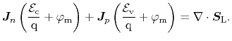
To consider the band gap alignment as typical in a heterostructure, the thermionic emission or thermionic field emission interface models must be used.

$\displaystyle J_\ensuremath{\mathrm{n1}}$ $\displaystyle =$ $\displaystyle J_\ensuremath{\mathrm{n2}}$ (4.58)
$\displaystyle J_\ensuremath{\mathrm{n2}}$ $\displaystyle =$ $\displaystyle \mathrm{q}v_\ensuremath{\mathrm{n2}} n_2 - \mathrm{q}v_\ensuremat...
...nsuremath{\mathrm{k}}_\ensuremath{\mathrm{B}}T_\ensuremath{\mathrm{n1}}}\right)$ (4.59)
$\displaystyle S_\ensuremath{\mathrm{n2}}$ $\displaystyle =$ $\displaystyle S_\ensuremath{\mathrm{n1}} - \frac{1}{\mathrm{q}} (\Delta \ensure...
...\ensuremath{\mathcal{E}}_{\ensuremath{\mathrm{c}}}}) J_\ensuremath{\mathrm{n2}}$ (4.60)
$\displaystyle S_\ensuremath{\mathrm{n2}}$ $\displaystyle =$ $\displaystyle -2\ensuremath{\mathrm{k}}_\ensuremath{\mathrm{B}}\left( T_\ensure...
...th{\mathrm{k}}_\ensuremath{\mathrm{B}}T_\ensuremath{\mathrm{n1}}}\right)\right)$ (4.61)

(4.58) guarantees the particle conservation at the interface. (4.60) relates the energy and current fluxes on both sides of the interface. The second term corresponds to the conversion of potential energy into kinetic energy, when the electrons descend the step $ \Delta\ensuremath{\ensuremath{\mathcal{E}}_{\ensuremath{\mathrm{c}}}}-\delta\ensuremath{\ensuremath{\mathcal{E}}_{\ensuremath{\mathrm{c}}}}$. (4.60) describes the thermionic emission across the energy barrier by relating the interface current to the quasi-Fermi level on both sides of the interface [134,282]. The exponential factor in (4.59) and (4.61) shows that only the fraction of the total electron concentration on Side 1, which is energetically above the barrier, is able to cross the potential step. In both (4.59) and (4.61) the same emission velocities occur:

$\displaystyle v_\ensuremath{\mathrm{ni}}(T_\ensuremath{\mathrm{ni}})=\sqrt{\fra...
...suremath{\mathrm{B}}T_\ensuremath{\mathrm{ni}}}{\pi m_\ensuremath{\mathrm{i}}}}$ (4.62)

Tunneling can be included in this model by assuming that the tunnel effect lowers the barrier $ \Delta\ensuremath{\ensuremath{\mathcal{E}}_{\ensuremath{\mathrm{c}}}}-\delta\ensuremath{\ensuremath{\mathcal{E}}_{\ensuremath{\mathrm{c}}}}$:

$\displaystyle \delta\ensuremath{\ensuremath{\mathcal{E}}_{\ensuremath{\mathrm{c...
...perp 2}}>0 0, & \quad E_\ensuremath{\mathrm{\perp 2}}\le 0 \end{array}\right.$ (4.63)

The barrier lowering $ \delta\ensuremath{\ensuremath{\mathcal{E}}_{\ensuremath{\mathrm{c}}}}$ depends on the electric field orthogonal to the interface $ E_\ensuremath{\mathrm{\perp 2}}$ and the effective tunneling length $ d_\ensuremath{\mathrm{tun}}$. The latter is material dependent: for Al $ _\ensuremath{\mathrm{0.2}}$Ga $ _\ensuremath{\mathrm{0.8}}$As/In $ _\ensuremath{\mathrm{0.2}}$Ga $ _\ensuremath{\mathrm{0.8}}$As it is estimated to 7 nm [283] and for Al $ _\ensuremath{\mathrm{0.25}}$Ga $ _\ensuremath{\mathrm{0.75}}$N/GaN to 3 nm [138].


S. Vitanov: Simulation of High Electron Mobility Transistors