As one can see in Table 5.1 the straight forward copy of conventional design, as was done with the flip-flop, is the worst choice.
The operation temperature is low, because the capacitors C0 which cross
connect both inverters have to be about a factor three bigger than the
capacitance of the tunnel junctions. This increases the capacity of the
quantum dots. The next best choice is the ring memory, ring-trap memory or MTJ
memory. All three are similar in design idea. But the MTJ
memory has twice as high an operation temperature. This can be understood
as follows. To introduce an error in the MTJ memory, at least one electron
has to tunnel from the quantum dot QD all the way to ground. That is, it has
to pass six tunnel junctions in our example. In the case of the ring memory
two electrons have to tunnel only through a single junction to change the
state of the cell, because once two electrons tunneled in the same direction
it is energetically favorable for the third electron to tunnel too. Thus
the MTJ memory has a bigger barrier against thermal fluctuations. In the
case of ring-trap memory thermal fluctuations introduce charge oscillations
even when no electrons are stored in the ring. This could trigger
Coulomb oscillations in the read-out SET transistor. That is why the operation temperature is
equal to the ring memory. However the read-out circuit can be
improved, by adding a filter. Thermal fluctuations are uncorrelated, but the
charge shifts due to a pulsed read-out voltage
![]() have a
specific frequency which could be filtered out. With this added
complexity the operation temperature should be improved
considerably.
have a
specific frequency which could be filtered out. With this added
complexity the operation temperature should be improved
considerably.
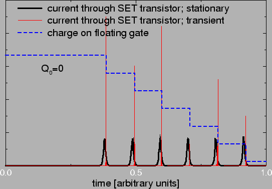
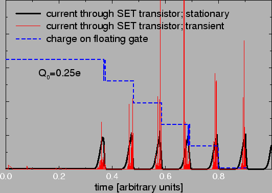
To show the random background charge independence of the Q0-independent
memory
of Fig. 5.12, we give in Fig. 5.15 the
current through the SET transistor for zero background charge and in
Fig. 5.16 the current for non-zero background charge.
 |
 |
An important issue for the fabrication and the achievable integration density
(bits/
![]() )
is the
complexity and
size of the various memory cells.
The SET flip-flop shows a high complexity with 10 elements (6 tunnel
junctions and 4 capacitors) with varying element parameters, or in the case
of the complementary design even 14 elements (8 tunnel junctions and 6
capacitors). Ring memory, ring-trap memory, and multi-tunnel-junction memory,
with 12, 13, and 7
elements respectively, are simpler in design. Their elements have similar
parameters and the interconnection is considerably less complex. Especially
in the case of the multi-tunnel-junction memory the connection problem is
considerably reduced, since only one island has to be connected to the
outside, and the number of tunnel junctions is not crucial. The
Q0-independent memory has only 4 elements (2 tunnel junctions, a floating
gate and a port to the floating gate) plus a FET sense amplifier which can
be responsible for many memory cells. The simplest design is the multi-island
memory cell which needs a small area of granular film and a drain, source and
gate electrode.
)
is the
complexity and
size of the various memory cells.
The SET flip-flop shows a high complexity with 10 elements (6 tunnel
junctions and 4 capacitors) with varying element parameters, or in the case
of the complementary design even 14 elements (8 tunnel junctions and 6
capacitors). Ring memory, ring-trap memory, and multi-tunnel-junction memory,
with 12, 13, and 7
elements respectively, are simpler in design. Their elements have similar
parameters and the interconnection is considerably less complex. Especially
in the case of the multi-tunnel-junction memory the connection problem is
considerably reduced, since only one island has to be connected to the
outside, and the number of tunnel junctions is not crucial. The
Q0-independent memory has only 4 elements (2 tunnel junctions, a floating
gate and a port to the floating gate) plus a FET sense amplifier which can
be responsible for many memory cells. The simplest design is the multi-island
memory cell which needs a small area of granular film and a drain, source and
gate electrode.
Considering the multi-island memory design, cell sizes of 50 nm ![]() 50 nm and below are possible, which would result in an integration
density of
50 nm and below are possible, which would result in an integration
density of
![]() bits/
bits/
![]() .
.
 |