Ion implantation is the primary technology to introduce doping atoms into a semiconductor wafer to form devices and integrated circuits [17,7]. This low-temperature process uses ionized dopants which are accelerated by electric fields to high energies and are shot into the wafer. The main reason in applying this technique is the precision with which the amount and position of the doping can be controlled. Dopant ions can be masked by any material which is thick enough to stop the implant as well as by existing device structures, which is referred to as self-aligned implants. After the implantation process the crystal structure of the semiconductor is damaged by the implanted particles and the dopants are electrically inactive, because in the majority of cases, they are not part of the crystal lattice. A subsequent thermal annealing process is required to activate the dopants and to eliminate the produced crystal damage.
Continuous growth and dominance of CMOS technology has directly resulted in the growth of ion implantation applications [17]. Leading edge CMOS processes which are used to fabricate a modern microprocessor require up to twenty ion implants per wafer. The doping requirements span several orders of magnitudes in both, energy and dose, for a wide range of dopant masses. An important implantation application for CMOS processing is, for instance, to form the source/drain regions in the substrate. Downscaling of MOS transistor dimensions requires the reduction of the source/drain junction depth to compensate the influence of the shorter channel length on the threshold voltage [7]. The subsequent application of an enhanced annealing process step like the flash-assist RTA (rapid thermal annealing) technique leads to a very limited diffusion which barely changes the as-implanted doping profiles and junction depth [26]. The distribution of dopants in the final device is therefore mainly determined by the ion implantation step, whereby channeling of implanted ions, which results from the regular arrangement of atoms in the silicon crystal structure, plays a major role.
![\includegraphics[width=.78\linewidth]{figures/iconc}](img95.png)
|
The intrinsic carrier concentration can be calculated from equations (2.6), (2.8), and (2.9) according to
|
![\includegraphics[width=.54\linewidth]{figures/intrinsic}](img108.png)
|
![\includegraphics[width=1.\linewidth]{figures/dopant-comb}](img109.png)
|
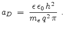
In processing of modern semiconductor devices, doping refers to the process of introducing impurity atoms into a semiconductor wafer by ion implantation. The purpose of semiconductor doping is to define the number and the type of free charges in a crystal region that can be moved by applying an external voltage. The electrical properties of a doped semiconductor can either be described by using the ``bond'' model or the ``band'' model. When a semiconductor is doped with impurities, the semiconductor becomes extrinsic and impurity energy levels are introduced. In Fig. 2.4 the bond model is used to show that a tetravalent silicon atom (group IV element) can be replaced either by a pentavalent arsenic atom (group V) or a trivalent boron atom (group III). When arsenic is added to silicon, an arsenic atom with its five valence electrons forms covalent bonds with its four neighboring silicon atoms. The fifth valence electron has a relatively small binding energy to its arsenic host atom and can become a conduction electron at moderate temperature. The arsenic atom is called a donor and a donor-doped material is referred to as an n-type semiconductor. Such a semiconductor has a defined surplus of electrons in the conduction band which are the majority carriers, while the holes in the valence band, being few in number, are the minority carriers. In a similar way, Fig. 2.4 demonstrates the behavior, if a boron atom with its three valence electrons replaces a silicon atom, an additional electron is ``accepted'' to form four covalent bonds around the boron, and a hole carrier is thus created in the valence band. Boron is referred to as an acceptor impurity and doping with boron forms a p-type semiconductor. The dopant impurities used in controlling the conductivity type of a semiconductor usually have very small ionization energies, and hence, these impurities are often referred to as shallow impurities. The energy required to remove an electron from a shallow donor impurity such as arsenic, phosphorus, and antimony can be estimated based on the Bohr model of the hydrogen atom [30,31]. The ionization energy of hydrogen is given by
Shallow acceptor impurities in silicon and germanium are boron, aluminium,
gallium, and indium. An acceptor is ionized by thermal energy and a mobile
hole is generated. On the energy band diagram, an electron rises when it
gains energy, whereas a hole sinks in gaining energy. The calculation of
the ionization energy for acceptors is similar to that for donors, it can
be thought that a hole is located in the central force field of a negative
charged acceptor. The calculated ionization energy for acceptors, measured
from the valence band edge, is
![]() in silicon and
in silicon and
![]() in germanium. The used approach for the calculation
of the ionization energy is based on a hydrogen-like model and the effective
mass theory. This approach does not consider all influences on the
ionization energy, in particular it cannot predict the ionization energy
for deep impurities. However, the calculated values do predict the correct
order of magnitude of the true ionization energies for shallow impurities.
The ionization energy for shallow impurities can also be calculated by
means of the density functional theory (DFT). In [32] both
approaches are compared to experimental data. The results obtained by the
DFT calculation are only for some impurities slightly more accurate than
the simple approach. Table 2.2 presents the measured ionization
energies for various donor and acceptor impurities in silicon and germanium.
in germanium. The used approach for the calculation
of the ionization energy is based on a hydrogen-like model and the effective
mass theory. This approach does not consider all influences on the
ionization energy, in particular it cannot predict the ionization energy
for deep impurities. However, the calculated values do predict the correct
order of magnitude of the true ionization energies for shallow impurities.
The ionization energy for shallow impurities can also be calculated by
means of the density functional theory (DFT). In [32] both
approaches are compared to experimental data. The results obtained by the
DFT calculation are only for some impurities slightly more accurate than
the simple approach. Table 2.2 presents the measured ionization
energies for various donor and acceptor impurities in silicon and germanium.
|
For shallow donors, it can be assumed that all donor impurities are ionized at room temperature. A donor atom which has released an electron becomes a positive fixed charge. The electron concentration under complete ionization is given by
![\includegraphics[width=.78\linewidth]{figures/nconc}](img141.png)
|
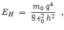
If donor and acceptor impurities are introduced together, the impurity present in a higher concentration determines the type of conductivity in the semiconductor. The Fermi level must adjust itself to preserve charge neutrality. Overall charge neutrality requires that the negative charges (electrons and ionized acceptors) must be equal to the total positive charges (holes and ionized donors):
![\resizebox{0.7\linewidth}{!}{\rotatebox{0}{\includegraphics[clip]{figures/electron}}}](img150.png)
|
Generally, the magnitude of the net impurity concentration
![]() is larger than the intrinsic carrier concentration
is larger than the intrinsic carrier concentration ![]() and the relationships
for
and the relationships
for ![]() and
and ![]() can be simplified to
can be simplified to
Fig. 2.6 shows the electron concentration in doped silicon with
![]() as a function of the
temperature [29].
At low temperatures the thermal energy in the crystal is not sufficient to
ionize all available impurities. Some electrons are ``frozen'' at the donor
level and the electron concentration is less than the donor concentration.
As the temperature is increased, the condition of complete ionization is
reached,
as a function of the
temperature [29].
At low temperatures the thermal energy in the crystal is not sufficient to
ionize all available impurities. Some electrons are ``frozen'' at the donor
level and the electron concentration is less than the donor concentration.
As the temperature is increased, the condition of complete ionization is
reached,
![]() .
As the temperature is further increased, the electron concentration remains
essentially the same over a wide temperature range. This region is called
extrinsic. As the temperature is increased further, we reach a point where
the intrinsic carrier concentration becomes comparable to the donor
concentration. Beyond this point the semiconductor becomes intrinsic.
The temperature at which the semiconductor becomes intrinsic depends on the
impurity concentration and the bandgap value. It can be obtained from
Fig. 2.3 by setting the impurity concentration equal to
.
As the temperature is further increased, the electron concentration remains
essentially the same over a wide temperature range. This region is called
extrinsic. As the temperature is increased further, we reach a point where
the intrinsic carrier concentration becomes comparable to the donor
concentration. Beyond this point the semiconductor becomes intrinsic.
The temperature at which the semiconductor becomes intrinsic depends on the
impurity concentration and the bandgap value. It can be obtained from
Fig. 2.3 by setting the impurity concentration equal to ![]() .
.
Ion implantation is a process whereby a focused beam of ions is directed towards a target wafer. Ionized particles are used in this process, because they can be accelerated by electric fields and separated by magnetic fields in an easy way in order to obtain an ion beam of high purity and well-defined energy. The ions have enough kinetic energy that they can penetrate into the wafer upon impact. The basic features of an ion implanter for doping semiconductors and the need to anneal the implant were patented by Shockley in 1957 [33]. The accelerators developed for nuclear physics research and isotope separation provided the technology from which ion implanters have been developed and the specific requirements of the semiconductor industry defined the evolution of the architecture of these small accelerators [34]. The next section describes some key elements of a modern ion implanter like the ion source and the beam transport system as well as a technique to achieve uniform doping over large wafers. The wafers are processed one at a time or in batches and are moved in and out of the vacuum by automated handling systems. The productivity of an ion implanter is of economic importance and there is continuing need to increase the usable beam current especially at low energies.
![\resizebox{0.9\linewidth}{!}{\rotatebox{0}{\includegraphics[clip]{figures/source}}}](img159.png) |
The ion source in an implanter must be capable of producing stable beams of the common dopants such as boron, phosphorus, arsenic, antimony, and indium. A beam current of up to 30mA and a lifetime of more than 100h before failure are required for cost effective productivity [34]. Among several different sources that have been developed the Bernas source with an indirectly heated cathode has become the source of choice for almost all implanters built today, and each manufacturer has developed a specialized design for their equipment [35]. Fig. 2.7 shows a typical example of this ion source. The ionizing electrons oscillate between the indirectly heated cathode and an anticathode and are confined by the magnetic field of a small electromagnet. The plasma density and the shape of the exit aperture of the ion source in combination with the extraction electrodes are important elements in the beam line since the quality and density of the ion beam entering the analyzing magnet system are determined in this region. A detailed discussion of extraction geometries can be found in a review by Hollinger [36], and of the beam transport system by Rose and Ryding [34].
When ion implantation was first adopted for doping semiconductors it was not realized what a large range of capabilities would ultimately be needed. Today, different machine types are used to cover the entire range of both energies and beam currents required for semiconductor fabrication. The machines can be grouped in medium current, high current, high energy implanters, and specialized implanters, for example, the oxygen implanter for SIMOX (separation by implantation of oxygen) technology [38].
Almost all the medium-current implanters which deliver beam currents in the range
of a few mA incorporate the concept of hybrid scanning by combining a beam scan
and a one-axis mechanical wafer scan. Fig. 2.8 shows an example of a
modern medium-current implanter from Nissin Corp. for 300mm wafers which can be
employed for the 45nm technology and beyond [37]. The ion beam is
generated in the ion source, mass analyzed at the analyzing magnet, accelerated
or decelerated at the acceleration column, energy filtered at the final energy
magnet, swept by the beam sweep magnet, and then collimated through the collimator
magnet. This implanter uses a one-dimensional hybrid scan, where the ion beam is
scanned and collimated by magnetic fields in horizontal direction and the wafer
is then mechanically scanned in vertical direction. The typical energy range
covered is between about 3keV and 250keV for singly charged ions. Using double or
triple charged ions extends the energy range to approximately 750keV.
Several manufacturers produce machines of this type and they are widely employed,
because they satisfy many of the lower doping requirements for devices, they
have a wide energy range and wafer throughputs as high as 450 wafers/h can be
achieved [37].
When source/drain implants requiring doses of 10![]() ions/cm
ions/cm![]() became
important, high-current implanters capable of beam currents larger than 10mA were
developed to allow fast processing of wafers. The decreasing junction depth
is creating a challenge for high-current implanters because below a few keV it
is difficult to obtain reasonably high beam currents [34].
became
important, high-current implanters capable of beam currents larger than 10mA were
developed to allow fast processing of wafers. The decreasing junction depth
is creating a challenge for high-current implanters because below a few keV it
is difficult to obtain reasonably high beam currents [34].
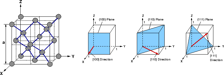
Channeling of implanted ions results from the regular arrangement of silicon
atoms in rows and planes in crystalline silicon. The silicon crystal has a
diamond structure, where each silicon atom is covalently bonded to four other
silicon atoms in a tetrahedral arrangement. This configuration belongs to the
face-centered cubic (FCC) crystal system with silicon atoms in all corners of
a cube, in the center of each cube face, and at four interstitial positions
within the cube, as shown in Fig. 2.9. The unit cell of the silicon
crystal with its lattice constant ![]() of 5.4307
of 5.4307
![]() at
at
![]() C defines the channels in silicon, where complex channeling behavior
can arise from this relatively simple arrangement of atoms.
C defines the channels in silicon, where complex channeling behavior
can arise from this relatively simple arrangement of atoms.
The Miller indices are commonly used to define planes of atoms and directions in the crystal The Miller indices
There are some additonal important points concerning the Miller index notation.
In the FCC crystal structure, a direction that has the same ![]() ,
, ![]() ,
, ![]() values
in its Miller indices as a plane is perpendicular to that plane. Thus,
values
in its Miller indices as a plane is perpendicular to that plane. Thus, ![]() ,
,
![]() , and
, and ![]() directions are perpendicular to
directions are perpendicular to ![]() ,
, ![]() , and
, and
![]() planes, as demonstrated in Fig. 2.9. There are directions and
planes that are identical with respect to physical properties like channeling.
For example, the directions
planes, as demonstrated in Fig. 2.9. There are directions and
planes that are identical with respect to physical properties like channeling.
For example, the directions ![]() ,
, ![]() ,
, ![]() ,
,
![]() , etc.
are all equivalent and referred to as
, etc.
are all equivalent and referred to as
![]() directions, while
the corresponding group of equivalent planes is designated as
directions, while
the corresponding group of equivalent planes is designated as ![]() planes.
planes.
![\resizebox{0.95\linewidth}{!}{\rotatebox{0}{\includegraphics[clip]{figures/ch-persp}}}](img189.png) |
Channeling is a significant phenomenon for implantation energies from 1keV up to several MeV. In the lower energy regime a larger deflection of an ion occurs even when the ion is traveling near the center of the channel [40]. This behavior is a direct consequence of the fact that the effective radius of silicon atoms along the channel increases as the ion energy is reduced. At a low enough energy the efective radii of the silicon atoms defining the channel become large enough to block that channel. Channeling can be reduced by a screening layer or by pre-amorphization. An amorphous layer, preferable silicon dioxide, can be deposited on the crystalline substrate to scatter the implanted ions. The pre-amorphization implant is performed before the desired implant in order to destroy the crystal structure of the substrate. Preferred ion species are silicon, germanium, or xenon. Both methods were investigated by simulation studies in [42].
The ion implantation process is mainly determined by the following five process
parameters:
The simplest semiconductor device is the pn-junction diode which can be easily
formed by ion implantation. Fig. 2.11 illustrates a typical n![]() /p-doping
profile which is formed by a p-well implant followed by the n
/p-doping
profile which is formed by a p-well implant followed by the n![]() -implant with
its maximum concentration near the surface.
-implant with
its maximum concentration near the surface.
|
![\resizebox{0.7\linewidth}{!}{\rotatebox{0}{\includegraphics[clip]{figures/dopants-color}}}](img200.png) |
![\resizebox{0.7\linewidth}{!}{\rotatebox{0}{\includegraphics[clip]{figures/dose}}}](img204.png) |
Fig. 2.13 shows the experimentally determined mean projected range ![]() of the most important dopant species as a function of the implantation
energy [43,44,16,45].
The
of the most important dopant species as a function of the implantation
energy [43,44,16,45].
The ![]() values are extracted from profiles measured by secondary ion mass
spectrometry (SIMS). Note that the
values are extracted from profiles measured by secondary ion mass
spectrometry (SIMS). Note that the ![]() data are averaged since SIMS data
exhibit a wide variation in results and only amorphous target materials are
commonly used to identify the
data are averaged since SIMS data
exhibit a wide variation in results and only amorphous target materials are
commonly used to identify the ![]() versus energy dependence.
In Fig. 2.13 it can be observed that the projected range of an ion is
larger for lower mass species. Therefore, boron has the largest projected range
of all investigated dopants, while antimony has the shortest projected range.
An exception of this rule can be observed for arsenic and antimony at lower
energies. This effect arises because the stopping power is dominated by nuclear
stopping in the low energy regime, while it is dominated by electronic stopping
in the high energy regime (as described in Section 3.1.3). Antimony has the maximum
position of the nuclear stopping power at a slightly higher energy than arsenic
which results in a lower stopping power below 5keV (inverse region) and a larger
versus energy dependence.
In Fig. 2.13 it can be observed that the projected range of an ion is
larger for lower mass species. Therefore, boron has the largest projected range
of all investigated dopants, while antimony has the shortest projected range.
An exception of this rule can be observed for arsenic and antimony at lower
energies. This effect arises because the stopping power is dominated by nuclear
stopping in the low energy regime, while it is dominated by electronic stopping
in the high energy regime (as described in Section 3.1.3). Antimony has the maximum
position of the nuclear stopping power at a slightly higher energy than arsenic
which results in a lower stopping power below 5keV (inverse region) and a larger
![]() , respectively.
, respectively.
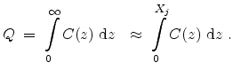
The total dose ![]() can be calculated by numerical integration of the dopant
concentration profile
can be calculated by numerical integration of the dopant
concentration profile ![]() from the wafer surface to at least the junction
depth
from the wafer surface to at least the junction
depth ![]() ,
,
The direction of incidence of the ion beam with respect to the wafer crystal
orientation is defined by the tilt and twist angle, as shown in Fig. 2.15.
The tilt is the angle between the ion beam and the normal to the wafer surface.
Wafer rotation or twist is defined as the angle between the plane containing the
beam and the wafer normal, and the plane perpendicular to the primary flat of
the wafer containing the wafer normal. The primary flat defines the orientation
of the silicon crystal, which is aligned to a ![]() direction in a
direction in a ![]() oriented wafer. The Miller index notation for describing directions and planes
in the crystal lattice system is explained in Section 2.2.2.
An appropriate tilt and twist can be used to minimize the channeling effect.
Large tilt angles are required in some implantation applications, for instance,
in halo implants.
oriented wafer. The Miller index notation for describing directions and planes
in the crystal lattice system is explained in Section 2.2.2.
An appropriate tilt and twist can be used to minimize the channeling effect.
Large tilt angles are required in some implantation applications, for instance,
in halo implants.
There are two silicon crystal orientations that are used in IC manufacturing,
![]() and
and ![]() silicon [28], which means that the crystal
terminates at the wafer surface on
silicon [28], which means that the crystal
terminates at the wafer surface on ![]() or
or ![]() planes, respectively.
Primarily because of the superior electrical properties of the
planes, respectively.
Primarily because of the superior electrical properties of the ![]() Si/SiO
Si/SiO![]() interface,
interface, ![]() wafers are dominant in manufacturing today.
wafers are dominant in manufacturing today.
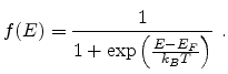
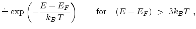
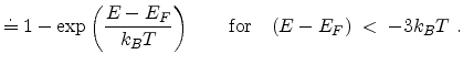
![\includegraphics[width=.55\linewidth]{figures/fermi}](img67.png)
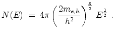

![$\displaystyle p\; =\; \int \limits_{-\infty}^{E_V} \left[1 - f(E)\right] N(E) \;\mathrm{d}E ,$](img91.png)
![$\displaystyle n_n =\; \frac{1}{2} \left[\; N_D - N_A + \sqrt{\left( N_D - N_A \right)^2 + 4 n_i^2}\; \right] \; ,$](img146.png)

![$\displaystyle p_p =\; \frac{1}{2} \left[\; N_A - N_D + \sqrt{\left( N_D - N_A \right)^2 + 4 n_i^2}\; \right] \; ,$](img148.png)

![\resizebox{0.7\linewidth}{!}{\rotatebox{0}{\includegraphics[clip]{figures/implanter}}}](img160.png)
![\resizebox{0.75\linewidth}{!}{\rotatebox{0}{\includegraphics[clip]{figures/junc-color}}}](img198.png)
![\resizebox{0.7\linewidth}{!}{\rotatebox{0}{\includegraphics[clip]{figures/range-color}}}](img203.png)
![\resizebox{0.7\linewidth}{!}{\rotatebox{0}{\includegraphics[clip]{figures/tilt-color}}}](img221.png)