Next: 2. Semiconductor Doping Technology
Up: Dissertation Robert Wittmann
Previous: List of Abbreviations and
Subsections
1. Introduction
Information technology (IT) is one of the most important
technologies, which has allowed to change the industrial society into an
information and knowledge based society. The electronic industry is the
largest industry in the world with a global sales volume of over
1 trillion US$ [1].
Microelectronics is the branch of electronics which deals with the
miniaturization of integrated circuits (ICs).
The evolution in microelectronics has resulted in complex System-on-a-Chip
(SoC) devices which combine logic and memory units consisting of hundreds of
millions of transistors packed on a single silicon chip. The production of
ultralarge scale integrated (ULSI) circuits was only possible due to the
CMOS (complementary metal oxide semiconductor) technology platform because
of low-power and scaling properties.
The workhorse of integrated circuits is the MOSFET (metal-oxide-semiconductor
field-effect transistor). This device is basically a switch where the electric
current in the silicon between the source and drain electrodes
is controlled by the potential of the gate electrode.
For four decades, the semiconductor industry has achieved continuous performance
enhancements by downscaling of the MOSFET device dimensions, as described
by Moore's Law. That is, the number of transistors per chip doubles
every eighteen months to two years.
In the last three years it has become clear that the conventional transistor
materials silicon and silicon dioxide have been pushed to fundamental material
limits. The International Technology Roadmap for Semiconductors (ITRS) defines
the current situation as material-limited device scaling [2]
which requires the introduction of new materials.
The incorporation of nitrogen into ultra-thin gate oxides to reduce the gate
leakage current and the use of strain to enhance the carrier transport in
silicon are two successful examples for the improvement of scaled bulk CMOS
devices. In the next several years, either extensions of bulk CMOS technology
or new approaches such as fully depleted SOI (silicon-on-insulator) and
multi-gate devices must further reduce the cost-per-function and increase
the performance of integrated circuits.
Technology Computer-Aided Design (TCAD) refers to the computer
simulation of semiconductor process and device technologies. TCAD tools play
a key role in the development of a new CMOS technology and they can help to
reduce the development time and costs. The combination of process and device
simulation tools in a TCAD framework enables analysis and optimization of
the influence of process parameters on the electrical characteristics of a
single device. Predictive modeling of a single process step in the IC
manufacturing process requires to include the underlying physics of that step.
An example of a very successful atomistic simulation approach is the Monte
Carlo modeling of the ion implantation process. Each ion trajectory is simulated
separately in this approach. In this way, an accurate prediction of the doping
profiles after ion implantation is achieved. For deep-submicron devices two-
and three-dimensional process simulations can provide a better insight than
measurement techniques and have become indispensible for the design of
advanced CMOS devices.
Rapid technology enhancements, introduction of new materials, and increasing
reliability problems caused by more and more shrinked device dimensions have
led to the situation that commercial TCAD tools cannot keep pace with numerous
newer developments. This situation becomes more critical in the field of
process simulation tools due to the existing diversity in the process steps.
The fabrication of a modern IC in the CMOS process involves hundreds of
sequential steps and can last up to 30 days of processing time [3].
The following basic process steps are used:
- Lithography: A lithography step is used to transfer the layout
information to the wafer. For instance, one photo mask can define the
source/drain areas for n-MOS transistors. Ultraviolet light is typically applied
to project the patterns defined by the mask to the photoresist layer which has
been deposited on the wafer surface. The structure defined by the mask remains
after the development process, if a positive photoresist is used.
- Deposition: Layers of various materials (semiconductors, metals,
insulators, photoresist) are deposited on the wafer surface during the IC
manufacturing process. Mainly two techniques are applied for deposition
processes: Physical Vapor Deposition (PVD) and Chemical Vapor
Deposition (CVD).
- Etching: Etching processes are used either to remove complete
material layers or to transfer the patterns in the photoresist layer (generated
by a lithography step) into the underlying layer. Etching can be performed by
a chemical attack (wet etching), by particles in a plasma chamber (dry etching),
or by a combination of both.
- Chemical Mechanical Polishing: A non-planar surface is produced
by process steps which modify the topography of the wafer (deposition, etching,
oxidation). The planarization for the next step is performed by Chemical
Mechanical Polishing (CMP).
- Oxidation: Silicon dioxide is used for isolation purposes in
devices and integrated circuits (e.g. shallow trench isolations between MOS
transistors) and as mask or scattering layers for ion implantation processes.
There are two silicon dioxide growth methods, dry and wet oxidation, depending
on whether oxygen or water vapor is used.
- Ion Implantation: This is the primary technology in IC
manufacturing to introduce impurities (dopant atoms) into semiconductors.
An ion implanter is used to accelerate the dopant ions to high energies and
to direct the beam of ions onto the wafer.
- Diffusion:
Dopant diffusion occurs during any thermal processing step either as an
intended or unwanted effect. Due to the requirement of very shallow
junctions in advanced devices rapid thermal annealing (RTA) processes
with very little diffusion (e.g. flash-assisted RTA or laser-anneal) are
used to repair the ion implantation induced damage in the crystal.
Figure 1.1:
Schematic cross-section of a final CMOS integrated
circuit with an interconnect structure of three metal layers (M1 - M3).
|
|
The CMOS process flow starts with a uniformly doped silicon wafer, and after
processing, the wafer contains hundreds of identical rectangular chips.
The IC fabrication can be subdivided into the following three major phases:
- The formation of the active devices close to the wafer surface
(front-end processing).
- The generation of the interconnect structure above the active
devices to form the integrated circuit (back-end processing).
- The chips on the wafer are electrically tested, separated, and
packaged.
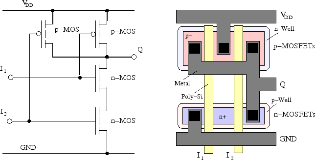
Figure 1.2:
Schematic of a CMOS NAND-gate (left) and its
layout (right) [4].
|
|
The final result of such a process flow is shown in Fig. 1.1. This modern
bulk CMOS structure is fabricated using a triple-well and a
dual-polysilicon gate process. Both MOS transistors are isolated
by an oxide-filled shallow trench isolation (STI).
CMOS technology integrates n- and p-channel MOS devices on the same chip.
An important characteristic of any CMOS circuit is that in either logic
state, at least one device in the series path from the power supply
to the ground is non-conductive. Therefore, the static power consumption
of the CMOS inverter is given by the leakage current of the off device.
A significant current flows only during the short transient period when
both devices change their state. Due to the low power dissipation requirement
in integrated circuits only the CMOS technology is currently used in advanced
IC manufacturing.
The NAND gate in Fig. 1.2 illustrates how additional n-MOS and
p-MOS devices can be added to the inverter circuit to realize more complex
logic functions. In the NAND circuit, the output Q will be grounded through
the two series n-MOS devices only, if both inputs I and I
and I are high.
The layout of the NAND-gate shows that the series connection of the two
n-MOS devices can be performed easily by a shared n
are high.
The layout of the NAND-gate shows that the series connection of the two
n-MOS devices can be performed easily by a shared n -doped region, and
the two p-MOS devices are connected by a shared p region.
It can be seen that the p-MOS device has a significantly larger area than
the n-MOS device. At least double the width of the n-MOS device is used
for the p-MOS due to the lower hole mobility in silicon. Finally, it
should be noted that a complex IC circuit can contain over
-doped region, and
the two p-MOS devices are connected by a shared p region.
It can be seen that the p-MOS device has a significantly larger area than
the n-MOS device. At least double the width of the n-MOS device is used
for the p-MOS due to the lower hole mobility in silicon. Finally, it
should be noted that a complex IC circuit can contain over  transistors, and each of them must work correctly.
The shrinking of MOS transistor dimensions is typically
performed by a scaling factor of 0.7 per each technology generation.
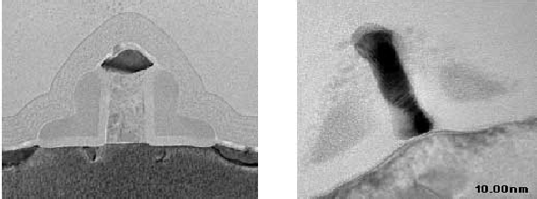
Figure 1.3:
Small devices with a gate length of 60nm
(left) and 10nm (right) [5,6]. The gate dielectric
thicknesses are 1.5nm and 0.8nm, respectively.
|
|
It has been demonstrated by Intel that a gate length of 10nm is possible in
experimental devices, as shown in Fig. 1.3. The ongoing downscaling
trend leads to some limitations and issues in modern CMOS technology, mainly
due to small-geometry effects. For instance, the punchthrough effect must be
suppressed in short channel devices [7], or the application
of ultra-thin gate dielectrics requires the incorporation of nitrogen into
the oxide, which in turn worsens the interfacial properties [8].
The issue of ultra-shallow source/drain junctions and their increased parasitic
resistance is discussed in Section 1.3.
An MOS transistor is considered short when the effective channel
length
 is comparable to the source/drain junction depletion
width [9]. In this case, the potential distribution in the channel
depends on both the normal and the lateral electric field in the device.
Experimentally, the short-channel effect is observed to degrade the subthreshold
characteristics and to reduce the threshold voltage
is comparable to the source/drain junction depletion
width [9]. In this case, the potential distribution in the channel
depends on both the normal and the lateral electric field in the device.
Experimentally, the short-channel effect is observed to degrade the subthreshold
characteristics and to reduce the threshold voltage  with decreasing
and increasing drain voltage
with decreasing
and increasing drain voltage  . When
is further reduced, the drain current finally cannot be turned off and the
gate has no control over the charge. The so-called punchthrough effect
poses a severe problem for miniaturized devices. Measures which are taken
to suppress this effect are retrograde wells and halo implants [7].
The purpose of these background doping profiles is to prevent the expansion
of the drain depletion region into the lightly doped transistor channel when
the device is switched on [10,11].
. When
is further reduced, the drain current finally cannot be turned off and the
gate has no control over the charge. The so-called punchthrough effect
poses a severe problem for miniaturized devices. Measures which are taken
to suppress this effect are retrograde wells and halo implants [7].
The purpose of these background doping profiles is to prevent the expansion
of the drain depletion region into the lightly doped transistor channel when
the device is switched on [10,11].
For devices with very short channels an additional effect occurs which leads
to increased leakage current. Due to the short distance between source and
drain, the potential at the drain contact reduces the peak value of the
energy barrier in the channel, which is called drain-induced barrier
lowering (DIBL). It leads to a decrease of the threshold voltage with
reduced channel length.
The required high channel doping to control short channel effects degrades
carrier mobility, lowers the drain current, and increases band-to-band tunneling
across the junction and gate-induced drain leakage (GIDL) [2].
Moreover, statistical fluctuation of channel dopants in small area devices
causes increasing variation of the value, posing difficulty in circuit
design while scaling the supply voltage.
As a consequence of the power-supply voltage being reduced much less
proportionally to the channel length
in practical scaling
(deviation from constant-field scaling), the lateral electric field is
increased in the device [9]. Carriers which move from the source
to the drain in such a turned-on MOS transistor can get enough energy to
cause impact ionization that generates electron-hole pairs in silicon and
surmount the interfacial energy barrier. The carriers injected into a gate
dielectric induce device degradation such as shift and reduced drain
current. Therefore, hot carrier injection (HCI) degradation
significantly reduces the transistor lifetime. The n-MOS transistor is more
sensitive to HCI than the p-MOS transistor, since electrons become hotter
than holes due to their higher mobility and the energy barrier is lower for
electrons compared to holes at the interface. This degradation effect was
considered as the major reliability problem in former technology generations,
in particular, if high electric fields were generated by constant-voltage
scaling. However, to solve this issue, drain engineering is used
to alleviate the peak of the lateral electric field located close to the
drain edge by modifying the drain doping profile through the introduction
of source/drain extension implants by a lower dose [7].
According to the CMOS scaling suggested in the ITRS roadmap [2],
the gate dielectric thickness should be reduced with every new device generation.
If the energy barrier between gate and semiconductor becomes too small, the
quantum-mechanical tunneling effect comes into play [12].
One solution to this effect is to use dielectric materials which have a higher
dielectric permittivity than silicon dioxide (SiO). These materials allow
to achieve a high physical thickness together with a small effective
oxide thickness (EOT). The EOT is defined as the thickness of a SiO layer
with equal capacitance. Since none of the alternative dielectric materials forms
a native oxide on silicon, a thin interfacial layer of SiO can hardly be
avoided. For a layer of SiO and a high-k dielectric, the EOT of the stacked
dielectric is
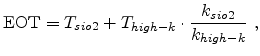 |
(1.1) |
where  and
and
 denote the thickness of the SiO and
high-k layer, and
denote the thickness of the SiO and
high-k layer, and  and
and
 are the respective permittivities,
respectively. With high-k dielectrics it is possible to retain good
control over the inversion charge even with physically thick dielectrics to
block tunneling currents. However, only nitrided gate oxides (SiON) are
currently used in state-of-the-art CMOS technologies because of critical
reliability issues of high-k dielectrics. On the one hand side, the incorporation
of nitrogen into the oxide reduces gate leakage, avoids boron penetration into
the dielectric, and improves HCI, and on the other hand side, it increases the
negative bias temperature instability (NBTI) effect [13].
The NBTI mechanism leads to a rapid shift of the transistor parameters (,
are the respective permittivities,
respectively. With high-k dielectrics it is possible to retain good
control over the inversion charge even with physically thick dielectrics to
block tunneling currents. However, only nitrided gate oxides (SiON) are
currently used in state-of-the-art CMOS technologies because of critical
reliability issues of high-k dielectrics. On the one hand side, the incorporation
of nitrogen into the oxide reduces gate leakage, avoids boron penetration into
the dielectric, and improves HCI, and on the other hand side, it increases the
negative bias temperature instability (NBTI) effect [13].
The NBTI mechanism leads to a rapid shift of the transistor parameters (,
 ) due to the buildup of charged interface traps during operation.
The NBTI reliability will be investigated for a 90nm technology node in
Section 5. CMOS scaling beyond the 45nm node requires the reduction of the
gate dielectric thickness down to an EOT of
) due to the buildup of charged interface traps during operation.
The NBTI reliability will be investigated for a 90nm technology node in
Section 5. CMOS scaling beyond the 45nm node requires the reduction of the
gate dielectric thickness down to an EOT of  nm which will either be
realized with SiON or high-k dielectrics.
nm which will either be
realized with SiON or high-k dielectrics.
Table 1.1:
Doping requirements from the 2005 ITRS roadmap [2].
| Year of introduction |
2005 |
2007 |
2010 |
| Technology node (nm) |
90 |
65 |
45 |
Channel doping concentration (cm ) ) |
 |
 |
 |
Sidewall spacer thickness  (nm) (nm) |
35.2 |
27.5 |
19.8 |
Extension junction depth  (nm) (nm) |
11 |
7.5 |
6.5 |
| Extension lateral abruptness (nm/decade) |
3.5 |
2.8 |
2.0 |
Contact junction depth  (nm) (nm) |
35.2 |
27.5 |
19.8 |
|
1.3 Trends in Doping Profiles for CMOS Technology
The ongoing scaling of device dimensions to increase packing density,
to increase operating speed, and to reduce power consumption has posed
difficult challenges for the doping of MOS transistors. As the channel
length is reduced in a scaled device the threshold voltage decreases
with the channel length (threshold voltage roll-off). The short channel
effect can be minimized if the source/drain junction depth is reduced
too. Table 1.1 shows the trend to very shallow junctions in
future CMOS technology nodes. Shallower junctions require the introduction
and activation of higher dopant concentrations to keep the resistance of
the source and drain regions small so that the drive current is maximized.
Table 1.1 also states that steeper lateral doping gradients
of the source/drain extension regions under the gate are necessary to
increase the device performance.
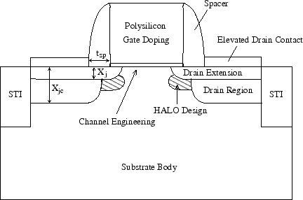
Figure 1.4:
Doping problems in extremely scaled MOS transistors.
|
|
Fig. 1.4 shows some major doping issues required to form an
advanced MOS structure.
Scaling of the contact area, junction depth, and contact silicide thickness
leads to an increase in parasitic resistance. A possible solution is to use
elevated source/drain contacts by selectively deposited silicon or germanium in
the contact region to make more silicon available for the silicide formation
process. In the polysilicon gate electrode the doping concentration has to be
pushed beyond known limits in order to limit the depletion layer thickness [2].
Halo implants (also known as punchthrough suppression or ``pocket'' implants)
avoid the punch-through between the source and drain through the bulk substrate
in short-channel devices. This implantation places the dopants just below the
active channel, adjacent to the source and drain regions, to precisely tailor
the well background doping there (see Fig. 1.4). Operating frequencies
above 1GHz have become possible for MOS transistors only due to the successful
introduction of halo implants [4]. Finally, channel engineering
with the doping profile of a modulated retrograde well structure will become
increasingly important for the optimization of various device parameters (e.g.
channel mobility, threshold voltage, source/drain junction capacitance, hot
carrier control, substrate current, soft error control) in future CMOS
technologies [7].
Virtually all doping profiles required for advanced CMOS processing are
accomplished by ion implantation. The reasons that ion implantation has
become the dominant doping technology in modern IC manufacturing are the
flexibility in selecting the dopant species, spatial location, and amount
of introduced dopant atoms within the device. This process provides a
very precise control and reproducibility for the desired dopant
distributions. Furthermore, the ion implantation process can be effectively
modeled on computers. The accurate simulation of implanted dopant
distributions in one-, two-, or three-dimensional structures requires only
a few input parameters and can reduce the development time and costs for
a new CMOS technology.
The three-dimensional ion implantation simulator MCIMPL-II (Monte
Carlo Implantation) [14] was used throughout
this work for the investigation of implanted doping profiles in silicon and
non-silicon materials. The simulator MCIMPL-II is based on a binary collision
approximation (BCA) [15] and will be described in detail in
Section 3. Beside MCIMPL-II, there are several ion implantation
simulators available on the market today, both commercial and academic ones.
Due to the high complexity inherent in BCA modeling, commercial ion implantation
simulators are often based on academic simulation codes. An analytical ion
implantation module is mostly used additionally to a Monte Carlo module to
allow a fast simulation of implantation profiles.
The Monte Carlo program TRIM (Transport of Ions in Matter)
was developed by Ziegler, Biersack and Littmark in 1985 [16], and then
rewritten to run on PCs [17]. This BCA program simulates the slowing
down and scattering of energetic ions in amorphous targets. The projectile
trajectory is statistically followed by randomly selecting a target atom, an
impact parameter, and a distance (mean free-flight-path). It was developed for
determining ion range and damage distributions as well as angular and energy
distributions of backscattered and transmitted ions.
The development of the MARLOWE simulator has been started in 1974 by Robinson
and co-workers [18,19]. The program uses a BCA technique
and considers crystalline target materials. The nuclear scattering is treated in
a precise manner by numerically evaluating the classical scattering integral
for realistic interatomic potentials. This calculation could be run only on a
mainframe computer because of the tremendous computational effort. UT-MARLOWE
is a highly modified MARLOWE code which was developed at the University of Texas
at Austin [20,21]. Recently, an interpolation scheme of scattering
events was developed to allow the implantation simulation of an arbitrary
species into crystalline silicon [22].
The program Crystal-TRIM was developed at the Forschungszentrum Rossendorf at
, based on the MARLOWE and TRIM codes. The current
version 04/1D simulates ion implantation into crystalline silicon, germanium
and diamond with up to 10 amorphous overlayers of arbitrary composition [24].
Not only atomic ions but also molecular ions may be considered. Dynamic simulation
of damage accumulation in crystalline substrates and the formation of amorphous
layers are possible. The simulator can be used to calculate implanted range and
damage distributions as function of depth. An efficient splitting algorithm
is employed in order to enhance the statistical accuracy of the simulation
results without considerable increase of computing time. It is particularly
useful, if channeling tails are of interest. Other versions of Crystal-TRIM
(for calculating two- and three-dimensional range and damage profiles) were
part of the process simulators TESIM, DIOS and FLOOPS, which were distributed
by ISE Integrated Systems Engineering AG, Z�rich. Now some of these simulators
are part of the TCAD software of Synopsys.
New materials have become more and more important in the development and
implementation of advanced CMOS technologies. Process-induced strained silicon
is currently used in the 65nm technology to enhance the drive current.
Biaxially strained silicon, silicon-germanium (SiGe) alloys with high Ge
concentrations or pure germanium offer larger intrinsic carrier mobilities
compared to process-induced strain, which can be exploited for channel
engineering.
The purpose of Chapter 2 is to provide a brief overview on semiconductor
doping technology. The first part of the chapter explains the theoretical
background of semiconductor doping and its impact on the electrical material
properties. The ion implantation technique for introducing dopant atoms into
semiconductors is presented in the second part.
Ion implantation is an extremely physical process, since the incoming
dopant ions make way for themselves by knocking the target atoms out of
their lattice sites. Chapter 3 starts with the description of the
fundamental physical models required for the Monte Carlo calculation of ion
implantation distributions. The following section of the chapter is focused
on the Monte Carlo ion implantation simulator MCIMPL-II [14].
The process simulation environment, the principle of operation, and the models
used for the trajectory calculation are described. Atomistic simulation
provides a better insight into the ion implantation process, for instance,
single ion trajectories can be visualized or the implantation induced vacancy
and interstitial concentration profiles are available. The improvement of the
simulation results by an advanced smoothing procedure is analyzed, and the
accomplishment of a three-dimensional application is demonstrated.
In Chapter 4 the implantation of boron and arsenic is studied in novel
crystalline materials such as SiGe alloys, germanium, and silicon-based
heterostructures as a replacement for bulk silicon. For this purpose, the ion
implantation simulator has been extended from silicon to these target materials
on the basis of experimental results. For the simulation of a new material,
the crystalline partner selection model has to be modified, the empirical
electronic stopping model has to be calibrated, and the displacement energy
for the damage generation has to be adapted. The investigations are focused
on the influence of strain, the germanium content in SiGe alloys, the damage
accumulation, and the channeling effect on the obtained doping profiles.
Negative bias temperature instability (NBTI) has emerged as a major reliability
concern for newer CMOS technologies [25]. In Chapter 5, the
impact of NBTI-driven degradation of transistor parameters on the lifetime of
a high-perfomance p-MOSFET is investigated. Experiments for different gate
voltages, frequencies, and duty cycles were performed to analyze the degradation
behavior for the key device parameters, and . The presently
leading reaction-diffusion (R-D) model is used for the numerical simulation of
interface trap generation based on the diffusion and accumulation of released
hydrogen in the gate oxide.
In Chapter 6, several simulation applications are presented. MCIMPL-II is
used for the three-dimensional simulation of ion implantation applications for
processing advanced MOS transistors and a high-speed photodetector.
The applicability of enhanced mobility materials for processing of improved
MOS devices with existing ion implantation equipment is shown. A calibrated
reaction-diffusion model is used to investigate the impact of NBTI-induced
transistor parameter degradation on the lifetime of a state-of-the-art SRAM cell
by numerical simulations.
Finally, Chapter 7 summarizes the thesis with some conclusions.
Next: 2. Semiconductor Doping Technology
Up: Dissertation Robert Wittmann
Previous: List of Abbreviations and
R. Wittmann: Miniaturization Problems in CMOS Technology: Investigation of Doping Profiles and Reliability
![\includegraphics[width=.86\linewidth]{figures/cmos-cross}](img41.png)