
 |
|
||||
BiographyHajdin Ceric was born in Sarajevo, Bosnia and Herzegovina, in 1970. He studied electrical engineering at the Electrotechnical Faculty of the University of Sarajevo and the Technische Universität Wien, where he received the degree of Diplomingenieur in 2000. In 2005 he received his PhD in technical sciences and in 2015 his venia docendi (habilitation) in microelectronics from the Technische Universität Wien. He is currently an Associate Professor at the Institute for Microelectronics. His research interests include finite element method modeling and simulation in microelectronics, application of machine learning in computer numerics, atomistic modeling in material science, electromigration in metals, and mechanical reliability of metals and semiconductors. In 2010 he was appointed the head of the Christian Doppler Laboratory for Reliability Issues in Microelectronics with two participating industrial partners: ams AG and Infineon Technologies Austria AG. Dr. Ceric participated in several European Community and FFG projects. In his research, Dr. Ceric has been closely cooperating with a company SOITEC, France, and research center imec, Belgium. He is a reviewer for several American Institute of Physics, Elsevier, and IEEE journals. Research Topics:Interconnect Reliability |
|||||
Electromigration-driven modification of polycrystalline metal structure
Electromigration (EM) as a physical phenomenon has been investigated for decades as a mechanism behind the degradation and failure of metallic interconnects. Initially a critical reliability issue for aluminum and later for copper interconnects, companies and research institutions have invested significant resources to understand and overcome the challenges posed by electromigration. This effort has gradually improved EM reliability through modifications to Back-End-of-Line (BEoL) technological processes and the introduction of new interconnect metals, such as ruthenium and cobalt, virtually eliminating EM as a reliability issue for nano-interconnects. However, for significant portions of interconnects today, such as through-silicon vias (TSVs) and various redistribution layers (RDLs), integrated circuits still rely on copper, where EM remains a challenging issue, particularly in combination with mechanical stress. A potential solution to this challenge is engineering the grain boundary structure of polycrystalline copper. It has been shown that under the influence of external mechanical load, metals react by generating nano-twinned grain boundaries, which may subsequently improve both mechanical and EM reliability. Given that the effects of EM on the metal and its grain boundary structure are well understood today, it is plausible to investigate the extent to which EM can be used to modify and improve the grain boundary structure of interconnect metals. In our research, we employ a combination of molecular dynamics (MD) simulations and density functional theory (DFT) calculations to investigate the structural changes of grain boundaries under the influence of EM. A crucial preliminary step in this investigation is determining the EM force in the vicinity and within the grain boundary. This can be achieved through various analytical approximations that rely on calculating electron distribution using DFT. The figure illustrates an example of such a calculation, showing a significant reduction in EM force within the grain boundary.
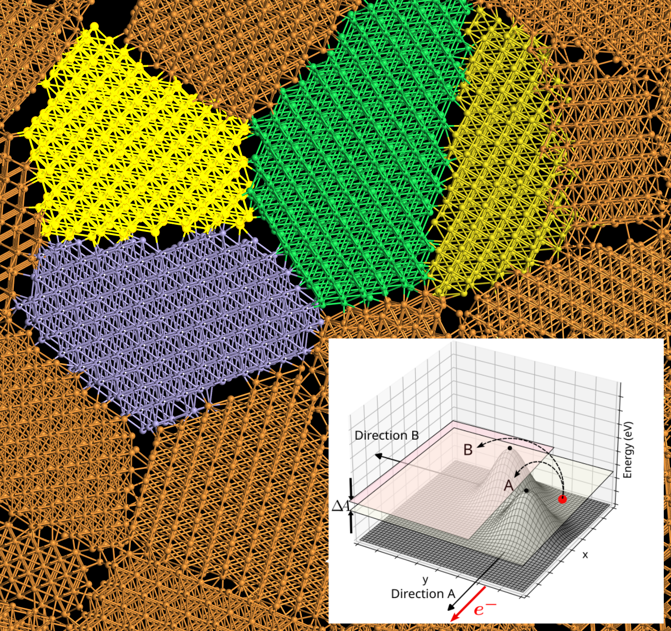
Fig. 1: EM force near and inside the grain boundary for different grain boundary to Fermi energy ratios (p = U/EF).