Atomistic Modeling
    t3kitt3kitt3kit
    • Home
    • TeachingOpen
      • Lehrveranstaltungen
      • Bachelorarbeiten
      • Masterarbeiten
      • Dissertationen
    • ResearchOpen
      • Activities
      • Computing Infrastructure
      • Characterization Lab
      • Annual Reviews
      • Public Projects
      • Conferences
    • PublicationsOpen
      • Books and Book Editorships
      • Papers in Journals
      • Contributions to Books
      • Conference Presentations
      • Scientific Reports
      • Patents
      • Habilitation Theses
      • PhD Theses
      • Master's Theses
    • SoftwareOpen
      • Software
      • Download
      • License Agreement
    • StaffOpen
      • Active Staff
      • Former Staff
    • About UsOpen
      • Contact Us
      • Join Us
      • Partners
      • Imprint
      • Corporate Design
      • Sitemap
    • News

    Atomistic Modeling

    Atomistic modeling is used in an increasing number of projects, either to supplement information from TCAD modeling (band structure, material parameters) or in its own right, to better understand material properties and material interfaces (defects, etc.). Some important examples are listed below.

    Material Modeling

    Fig. 1: Bandstructure of hBN as obtained from DFT

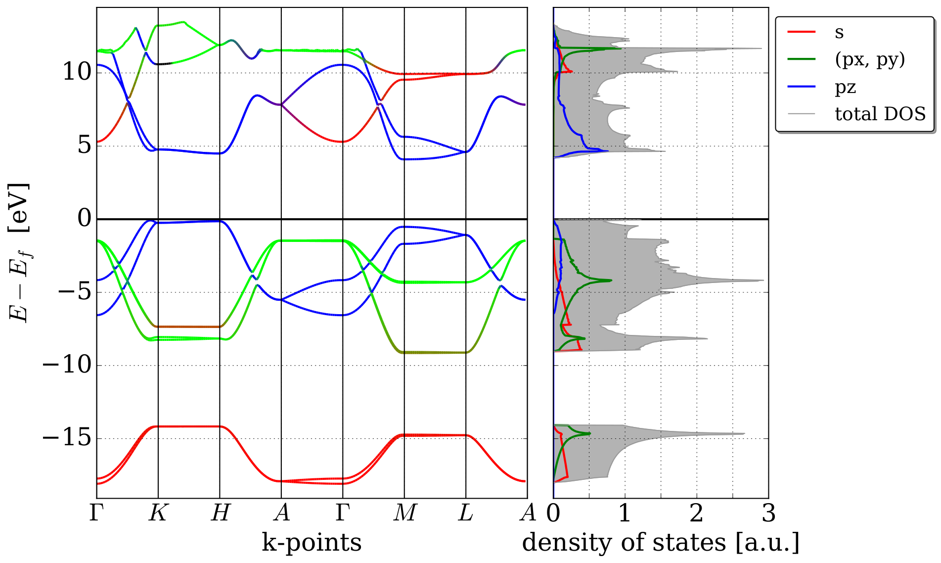
    DFT is used to calculate the bandstructure of various materials for use in classical and quantum mechanical transport codes. This is particularly useful for the new class of 2D materials where material parameters are not easily accessible experimentally, see Fig 1. In addition, the properties of interfaces are explored for various material combinations.

    Defect Modeling

    Fig. 2: Volatility of a hydroxyl E' center caused by the release of hydrogen following the neutralization of the defect. On the right, the potential energy surface extracted from DFT is shown.

    For reliability modeling, the properties of various point defects are thoroughly investigated using DFT. Recent investigations have shown that point defects in amorphous materials can have a multitude of possible states. One example is shown in Fig. 2, which demonstrates how hydrogen can be released from a hydroxyl E' center as soon as it becomes neutralized. Using DFT, the potential energy surfaces related to the various states are calculated, including nudged-elastic-band calculations to explore thermal barriers, which then form the basis for more efficient TCAD models.

    Electromigration Modeling

    Fig. 3: Calculated values of the effective valence (Z*) for the case of reciprocal densities of the copper grain boundariesof coincident sites equal to 5 and tilt angle of 53.1 degrees (210)

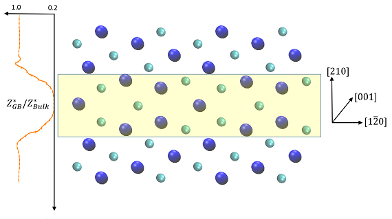
    The effective valence characterizes the susceptibility of the interconnect metal to electromigration and establishes a linear relationship between the electromigration force (with direct and electron wind components) and an external electric field. The applications of DFT, for metals carrying a steady state current, is of particular interest in calculation of the effective valence.

    DFT calculations are used in combination with the non-equilibrium Green's function method to obtain non-equilibrium electron densities which allows for the determination of the atomic electromigration force (and thus, the effective valence) through application of the Feynman-Hellman theorem.

    Contact

    Hajdin Ceric
    Metals

    Tibor Grasser
    Point defects

    Hans Kosina
    Band structure

    Key Publications

    Hydrogen-Related Defect Volatility
    with UC London

    Hydrogen-Related Point Defects in SiO2
    with UC London


    • Activities
      • Device Reliability
      • Device Simulation
      • 2D Materials and Devices
      • Magnetic and Spin Devices
      • Semiconductor Sensors
      • Classical and Quantum Transport
      • Process Simulation
      • Interconnect Reliability
      • Characterization
      • Mechanics of Microelectronics
      • Atomistic Modeling
      • High Performance Computing
    • Computing Infrastructure
    • Characterization Lab
    • Annual Reviews
    • Public Projects
    • Conferences

    Institute for Microelectronics
    Head: Univ. Prof. Dipl.-Ing. Dr. techn. Tibor Grasser
    Deputy Head: O. Univ. Prof. Dipl.-Ing. Dr. techn. Dr.h.c. Siegfried Selberherr
    Contact Us    |    Join Us    |    Imprint
    © E360 - Institute for Microelectronics 2018