Mechanics of Microelectronics
Mechanics of microelectronics systems represents an engineering challenge since it deals with structures at different geometric scales, material compositions, and functionalities. The focus of our work is on the mechanical behavior of multilayer structures, silicon wafers, and integrated microheaters.
Multilayer structures in microelectronics can mechanically fail due to three main degradation mechanisms: tensile rupture (fracture due to mechanical overloading), creep failure (damage caused by a long-lasting permanent load or stress), and fatigue (damage caused by cyclical loads or stresses). These mechanisms affect the multilayer structures simultaneously. The thermomechanical stress is the main source of mechanical degradation and failure related to cracking, delamination, ratcheting, and stress-induced voiding. Our primary research is focused on improving the reliability and mechanical stability of the microelectronic structures considering the above described failure phenomena. The general strategy for the reliability improvement is:
- Reducing the stress level in critical areas
- Increasing the stress threshold in critical areas
Both strategies may lead to a change in one, or a combination of, the following: the device geometry, the materials used, and the technological processing step applied.
Through-Silicon-Vias
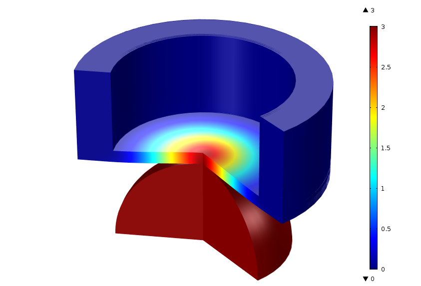
Two facts make the mechanical reliability studies of the through-silicon-via (TSV) structure particularly challenging. The first is that a TSV consists of a number of different materials layered against each other and the second is that these materials are combined in a way that they build geometrically complex interfaces and geometrical features which are small compared to the overall TSV dimension. In order to asses the mechanical reliability of TSV structures and predict the development of failures, three-dimensional (3D) simulations of mechanical stress distribution must be performed (Fig. 1). In addition to the mechanical stability, the electrical reliability of TSVs must be analyzed, which is done using electromigration models.
Silicon Wafers
The investigations leading to a better understanding of plastic deformation of silicon wafers, during thermal processing are of major interest to the microelectronics industry. Such investigations are intended to help predict plastic wafer warping and to aid in its reduction to acceptable level. The plastic deformation of silicon wafers is comprehensively described by the Haasen-Alexander-Sumino (HAS) model, which relates time-dependent creep strain to the dislocation density distribution inside the silicon wafer.
Integrated Sensors
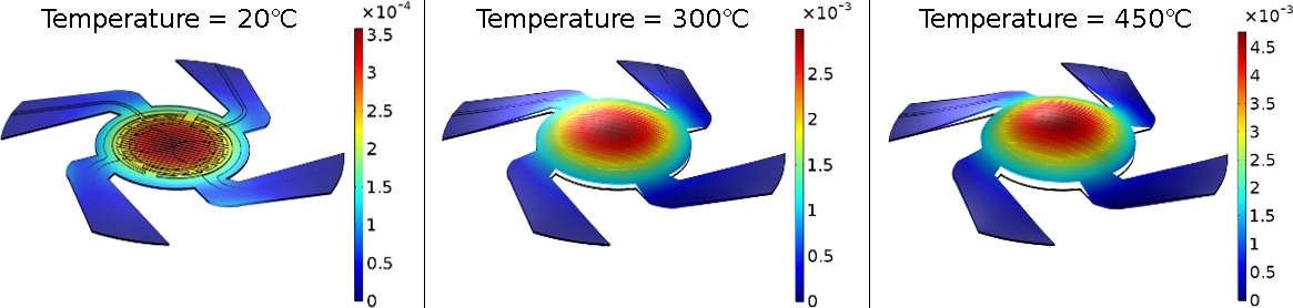
A further microelectronics application, which greatly benefits from mechanical simulations, is the integration of sensors which require a localized microheater. This microheater is fabricated on a suspended membrane, which comprises several layers including oxide, nitride, the microheater itself, and the sensing film. These types of structures are commonly used in pressure sensors, accelerometers, fingerprint sensors, gas sensors, and IR emitters, to name a few. With a combination of CMOS and MEMS fabrication techniques, researchers have successfully fabricated these structures, but due to the complexity in the layer stack and the frequent heating and cooling of the device to initiate sensing, mechanical stability is of upmost importance. In Fig. 2 we note the stress-induced deformation of a suspended membrane stack (SiO2/SiN/SiO2) while being heated from room temperature to 450°C.