 |
We approximate the sputter reactor flux by using an exponential function which is fitted to the angular distributions resulting from Monte-Carlo simulations of sputtering particle transport [18]. The detailed model for the sputter deposition including derivation of visibility conditions, particle distributions and simulations at arbitrary wafer positions is described in [19].
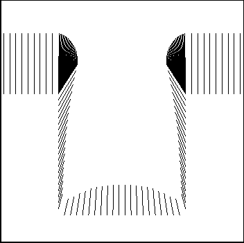
Fig. 9 shows a cross-section of calculated deposition rates for a three-dimensional simulation of TiN magnetron sputter deposition into a circular via. The dark area at the topmost corner shows the interpolation of the rates similar to the interpolation for the isotropic simulation.
|
Fig. 10 shows how the procedure described above is used for the
three-dimensional simulation of sputter deposition. The figure shows a via
located close to the edge of the wafer. The view angle of the sputter target
center is about 12![]() , therefore the main incidence direction of particles
is tilted resulting in the asymmetrical profile evolution. Fig. 11 shows the
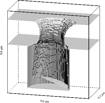
application of this model to the simulation of TiN magnetron sputter deposition.
A special thing to note is the formation of overhangs at the topmost convex
corner of the structure. The simulation clearly reveals the bulge formation
observed in the experimental SEM pictures. This is only possible with a special
treatment of the convex corners already presented in detail in [20].
, therefore the main incidence direction of particles
is tilted resulting in the asymmetrical profile evolution. Fig. 11 shows the
application of this model to the simulation of TiN magnetron sputter deposition.
A special thing to note is the formation of overhangs at the topmost convex
corner of the structure. The simulation clearly reveals the bulge formation
observed in the experimental SEM pictures. This is only possible with a special
treatment of the convex corners already presented in detail in [20].
![\begin{figure}\begin{center}
\par\psfrag{0}[rc]{\LARGE {0}}
\psfrag{1.8}[rc]{\LA...
...0.28\textwidth}{!}{\includegraphics{pH_10_bw.eps}}}
\par\end{center}\end{figure}](img27.gif) |
[<] [^] [>] [TOC] Prev: 3.2 Unidirectional Etching/Deposition Up: 3 Topography Algorithms Next: 3.4 Timings