|
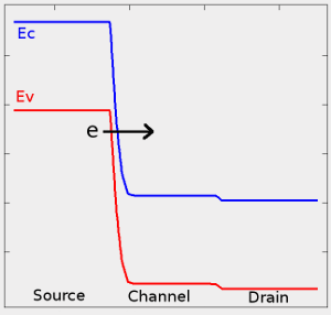
Power dissipation has become a limitation in scaling of modern integrated devices. Due to off-state leakage, MOSFETs are reaching their scaling limitation. In order to operate at lower power, devices are necessary that require lower voltage swing. Tunneling FET (TFET) structures have the potential to remove this limitation and can be designed to operate at sub 60 mV/dec subthreshold swing.
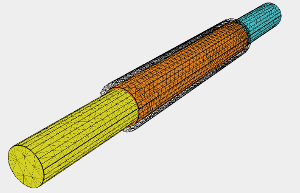
In order to continue with the miniaturization of devices and decrease in power, axial nanowire heterostructures are used for TFET designs, with transport along the axis of the nanowire (NW). Various material combinations and doping levels, that are integrateable with existing silicon technology, such as Si, Ge, SiGe NWs as well as Silicide and Germanide heterojunctions, are considered to build the p-i-n NW heterostructures. These structures rely on band to band tunneling for carrier transport.
Physical modeling of the devices is performed using the Vienna Schrödinger Solver (VSP). 3D structures are generated and meshed using an unstructured finite volume meshing scheme. The solution of Poisson's equation for the structures generates a potential energy profile through the device. The resulting potential distribution is used to calculate current contributions through different tunneling mechanisms.
In order to calculate the current through NW heterostructures, tunneling mechanisms must be modeled appropriately. These include direct tunneling, interband tunneling, phonon interaction and trap-assisted tunneling. Numerous methods are examined for computation of necessary effects. The Wentzel-Kramers-Brillouin (WKB) approximation provides estimated, simplified, closed form expressions for elastic interband tunneling. This applies to direct semiconductors, as phonon interaction is not considered. A more complete tunneling computation would involve a solution of the Non-Equilibrium Green's Function equations or Zener tunneling with phonon assisted tunneling.
Through numerical tunneling current studies, material, doping levels and strain, devices can be engineered for optimal performance. The current tunneling model incorporates 1D direct tunneling. Expansion of elastic and inelastic band to band tunneling processes is currently under development.
|