|
In the TCAD version of our Hot-Carrier Degradation (HCD) model we use a combination of different device simulators in order to achieve a reasonable trade-off between the accuracy and computational burden. First, the full-band Monte Carlo device simulator MONJU is employed to calculate the set of carrier distribution functions along the interface. Then, these distribution functions are used to calculate the carrier acceleration integral vs. the coordinate along the interface to eventually produce the trap density as a function of the coordinate. Finally, the interface state concentration calculated in this manner is used as input for our device simulator MINIMOS-NT to calculate the characteristics of the degraded device. The whole computational procedure is performed for each time step in order to evaluate the degradation of device characteristics against the stress time.
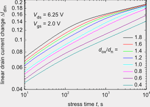
A "brute-force" approach to analyze the impact of device architecture variations on the behavior of the transistor degraded during hot-carrier stress may be performed in the following manner: at the initial step a set of topologically identical devices differing only in the value of the fluctuating parameter is generated. Then, for each particular device (with the unique value of the varying parameters) the whole above described procedure is applied. The results are then statistically processed by weighting with the distribution of the fluctuating quantity. However, due to the stochastic nature of the Monte Carlo approach, such a computational procedure would lead to an enormous computational burden. Instead, we use an analytical approach which is calibrated using the results obtained with the TCAD version of the HCD model. We vary an architectural parameter (in this example the oxide thickness) and for some reference values we apply the full TCAD model to obtain the exact dependences of the drain current vs. time. Then we interpolate parameters in the analytical formula for the acceleration integral in order to cover the whole range of the fluctuating parameter.
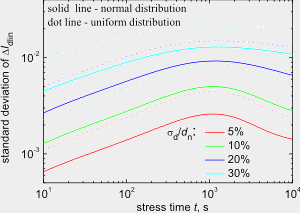
We have analyzed the impact of oxide thickness variations on the linear drain current change vs. time during hot-carrier stress. The calculations have demonstrated that the change in the drain current vs. time is rather sensitive to an oxide thickness change at short and moderate stress times (figure 1). For longer stress times, the difference between the drain current degradation obtained for different oxide thicknesses tends to vanish. This is because, during extended times, all Si-H bonds in the vicinity of the acceleration integral peak are predominately broken, independent of the real thickness. We have also calculated the mean value and the standard deviation (figure 2) of the drain current change as a function of time for different oxide thickness distributions, which confirms this tendency.
|