One of the problems researchers face is that the exact transition from crystalline silicon to amorphous silicon-dioxide and the possible defects are not totally clear. Chapter 3 gives an overview of the resent research results concerning this interface and its defects.
In this section the proposed physical mechanisms that lead to BTI are presented and their validity discussed.
![\includegraphics[width=10cm]{figures/nbti-stress-schematic}](img497.png)
|
![\includegraphics[width=\figwidth]{figures/meas-interval-new}](img498.png)
|
To extract the level of degradation the stress is interrupted several times for short measurement cycles. During these measurement intervals typically the threshold voltage is measured performing a gate voltage sweep while measuring the current at the slightly forward biased drain contact. The interface trap density can be extracted using the charge pumping (Section 4.1), DCIV (Section 4.2), or CV (Section 4.3) methods.
This is the basic experimental set-up which was formerly used to obtain NBTI data found in literature. The problem with this method is the strong recovery of NBTI induced damage during the first milliseconds or even microseconds after the stress is released. Figure 6.3 qualitatively illustrates the measurement error obtained due to the fast recovery of NBTI degradation. When the stress gate voltage is removed, a part of the degradation relaxes. As a consequence the measured degradation of figures of merit, such as the threshold voltage or the interface trap density, is strongly dependent on the delay between the end of the stress conditions and the time where the value of the degradation is measured. This fast transient effect has been shown by Ershov et al. in 2003 [91] and led to the development of advanced measurement methods as described below.
![\includegraphics[width=\figwidth]{figures/single-meas-point}](img499.png)
|
As only one drain current has to be obtained, instead of a range of drain currents for different gate biases, this approach is drastically faster and the error due to the fast recovery is reduced.
This technique still suffers from a measurement delay of some tens or hundreds of milliseconds. In order to completely remove the, normally unintentional, recovery during the measurement conditions on-the-fly measurement methods with zero delay have been proposed [93,94], which are discussed in the next sections.
One concern using this method might be the following: although the stress gate
voltage is never removed during measurement, biasing the drain contact with the
same voltage still leads to a drastic change of the electric field at the
![]() interface, especially close to the drain contact. As the electric
field has been found to be one of the major driving forces of NBTI degradation,
this change of the field will most likely lead to altered degradation behavior.
interface, especially close to the drain contact. As the electric
field has been found to be one of the major driving forces of NBTI degradation,
this change of the field will most likely lead to altered degradation behavior.
![\includegraphics[width=\figwidth]{figures/mos-surffield}](img502.png)
|
Figure 6.5 depicts the electric field at the
![]() interface of a
MOSFET biased at symmetric stress conditions with
interface of a
MOSFET biased at symmetric stress conditions with
![]() and
and
![]() V
and also with
V
and also with
![]() . It can be clearly seen that the electric
field component normal to the interface changes severely when applying a high
drain voltage. This might invalidate the main argument for this measurement
method, of not changing the degradation behavior during measurement.
. It can be clearly seen that the electric
field component normal to the interface changes severely when applying a high
drain voltage. This might invalidate the main argument for this measurement
method, of not changing the degradation behavior during measurement.
The amount by which the electric field is altered during measurement depends strongly on the exact device geometry, the doping concentrations, and also the stress bias. Appropriate simulations have to be made to evaluate the impact on the electric field before using this measurement for device qualification.
Another problem of this method is the high channel current during measurement. It can lead to additional degradation mechanisms due to hot carrier stress (Section 5.1), as hot carrier injection into the oxide.
For circuit design the threshold voltage is in most cases of more interest than the drain current in saturation. The next on-the-fly method extracts the threshold voltage while keeping the gate stress approximately constant.
Using this method, the source and bulk contacts are grounded while the drain
contact is slightly biased with typically ![]() mV. The stress at the gate
contact is permanently applied and superimposed with pulses which are small
compared to the stress voltage. With the small drain voltage, as compared to
the drain pulsed voltage method, neither the problem of the severely changing
interface electric field nor hot carrier degradation are imminent.
mV. The stress at the gate
contact is permanently applied and superimposed with pulses which are small
compared to the stress voltage. With the small drain voltage, as compared to
the drain pulsed voltage method, neither the problem of the severely changing
interface electric field nor hot carrier degradation are imminent.
The transconductance
![]() of the transistor, which is defined as the change in
drain current as a result of a change of gate voltage, can then be extracted as
of the transistor, which is defined as the change in
drain current as a result of a change of gate voltage, can then be extracted as
 |
(6.2) |
From this relation also the threshold voltage can then be extracted.
|
During stress tests it is often useful to measure the source, drain, and gate
currents,
![]() ,
,
![]() , and
, and
![]() . Devices which suffer from oxide breakdown
during stress can then be detected as
. Devices which suffer from oxide breakdown
during stress can then be detected as
![]() should stay very low and
should stay very low and
![]() should be approximately equal to
should be approximately equal to
![]() . Sudden changes in terminal voltages,
as seen in Figure 6.6, are not typical for NBTI and suggest an
additional degradation mechanism.
. Sudden changes in terminal voltages,
as seen in Figure 6.6, are not typical for NBTI and suggest an
additional degradation mechanism.
|
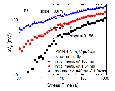
Figure 6.7 depicts data from [99] showing the apparent
threshold voltage shift over time in logarithmic scale. It can be seen that
for long delay times of 100ms at the initial measurement, the kink in the
power law is very pronounced. But as the initial measurement time is
drastically reduced to 1.04ms, and therefore the accuracy of this measurement
increased, the kink becomes less obvious. The authors showed that by assuming
a shift of the threshold voltage of 40mV even at the fast initial
measurement, and adding it to the following data they can achieve a clear
power-law with the time exponent of ![]() . This slope varies drastically
when the amount of initial degradation is not added and might explain the wide
spread of the data reported in literature.
. This slope varies drastically
when the amount of initial degradation is not added and might explain the wide
spread of the data reported in literature.
To conclude, not only the speed of the degradation measurements during stress is important in order to spot the fast transients during relaxation, but also the accuracy of the initial degradation measurement is of highest importance and can be improved by very high speed measurement methods [100].
|
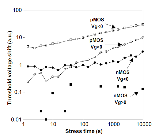
It has been reported that for NBTI degradation channel cold holes are important [101,86]. As the n-channel MOSFET biased into accumulation also has holes at the surface of the substrate, the threshold voltage shift should be similar to p-channel MOSFETs. Therefore, the lack of holes can not be the cause for the different degradation behavior.
Oxide traps are positively charged by hole trapping in both, the n- and
p-channel MOSFET. Therefore their contribution to a
![]() shift should be
comparable. The charge state of the interface traps, on the other hand side,
depends on the Fermi-level as pointed out in Chapter 3. The
threshold voltage of a MOSFET is reached when the surface of the substrate is
driven into weak inversion. Therefore the charge state at the
silicon-dielectric interface under inversion conditions is very important.
shift should be
comparable. The charge state of the interface traps, on the other hand side,
depends on the Fermi-level as pointed out in Chapter 3. The
threshold voltage of a MOSFET is reached when the surface of the substrate is
driven into weak inversion. Therefore the charge state at the
silicon-dielectric interface under inversion conditions is very important.
The Fermi-level at the interface of a p-channel MOSFET biased into inversion is
below the mid-gap energy. As Figure 6.9(a) illustrates, in this
regime the acceptor like trap levels are empty, and the donor like trap levels
are partially filled, assuming the trap energy levels to be symmetrically
aligned around mid-gap. The net charge resulting from this configuration is
positive and leads to a total interface charge for p-channel MOSFETs of
| (6.3) |
|
| (6.4) |
In p-channel MOSFETs, both, the interface and the oxide traps contribute to the threshold voltage shift. In n-channel devices the charge state of the interface traps reduces the shift introduced by the oxide traps and the effect of NBTI is therefore less pronounced in n-channel MOSFETs.
The activation energy for dissociation of P-H bonds is usually very high. Only in the depletion region the bonds are weakened and can be cracked more easily. During NBT stress a p-channel MOSFET is driven into inversion and a depletion region is formed in the substrate. In this region the hydrogen atoms can be dissociated and cause degradation at the interface. For positive stress no depletion region is formed. Therefore no hydrogen can be provided by dissociating P-H bonds, and the level of degradation is reduced.
In the n-channel MOSFET the substrate is typically doped with boron and hydrogen can only be supplied from B-H bonds. As their binding energy is much higher, also in depletion regions, n-channel MOSFETs are much less susceptible to bias instability, no matter which polarity the stress voltage has.
The Fermi-level of a p-type poly gate lies approximately at the valence band
edge
![]() while the Fermi-level of an n-type poly gate is located at the
conduction band edge energy
while the Fermi-level of an n-type poly gate is located at the
conduction band edge energy
![]() . For NBT stress the p-type poly gate
of the p-channel device is depleted while the n-type poly gate of the n-channel
device is driven into accumulation.
. For NBT stress the p-type poly gate
of the p-channel device is depleted while the n-type poly gate of the n-channel
device is driven into accumulation.
Oxide and interface charges (
![]() and
and
![]() ) generated by NBTI degradation
further shift the relevant gate voltages as described in
Section 2.2.1.
) generated by NBTI degradation
further shift the relevant gate voltages as described in
Section 2.2.1.
Due to this asymmetry for n- and p-type gate contacts, the oxide electric fields are not equal for a given gate voltage and at a given oxide electric field the gate voltages differ. This has to be considered when comparing the two types of transistors.
![\includegraphics[width=0.495\textwidth]{figures/brokengatedielectric}](img507.png)
![\includegraphics[width=0.495\textwidth]{figures/brokensd}](img508.png)
![\includegraphics[width=0.495\textwidth]{figures/pb-charge-small-nsub}](img514.png)
![\includegraphics[width=0.495\textwidth]{figures/pb-charge-small-psub}](img515.png)