Another application is the simulation of anisotropic wet etching. In [96], a model for anisotropic wet etching of silicon with potassium hydroxide (KOH) is described. The material transport to the surface can be neglected for this process. The surface velocity only depends on the crystallographic orientation of the surface, thus on the local surface normal ![]() . It is assumed that
. It is assumed that ![]() is given with respect to the crystallographic directions,
is given with respect to the crystallographic directions,
![]() ,
,
![]() , and
, and
![]() . Utilizing the crystallographic symmetries of silicon, it is possible to only consider the case
. Utilizing the crystallographic symmetries of silicon, it is possible to only consider the case
![]() . This allows the surface velocity to be approximated by
. This allows the surface velocity to be approximated by
Inserting these numerical values into (6.3) leads to a non-convex Hamiltonian for the LS equation. Hence, to obtain a stable solution, a non-convex scheme, such as the Lax-Friedrichs scheme, must be applied (see Section 3.2.2). For the simulations, presented in the following, the dissipation coefficients
![]() in (3.12) are all set to
in (3.12) are all set to
![]() . This value has been found through variation and selection of the value that gives the most accurate simulation results.
. This value has been found through variation and selection of the value that gives the most accurate simulation results.
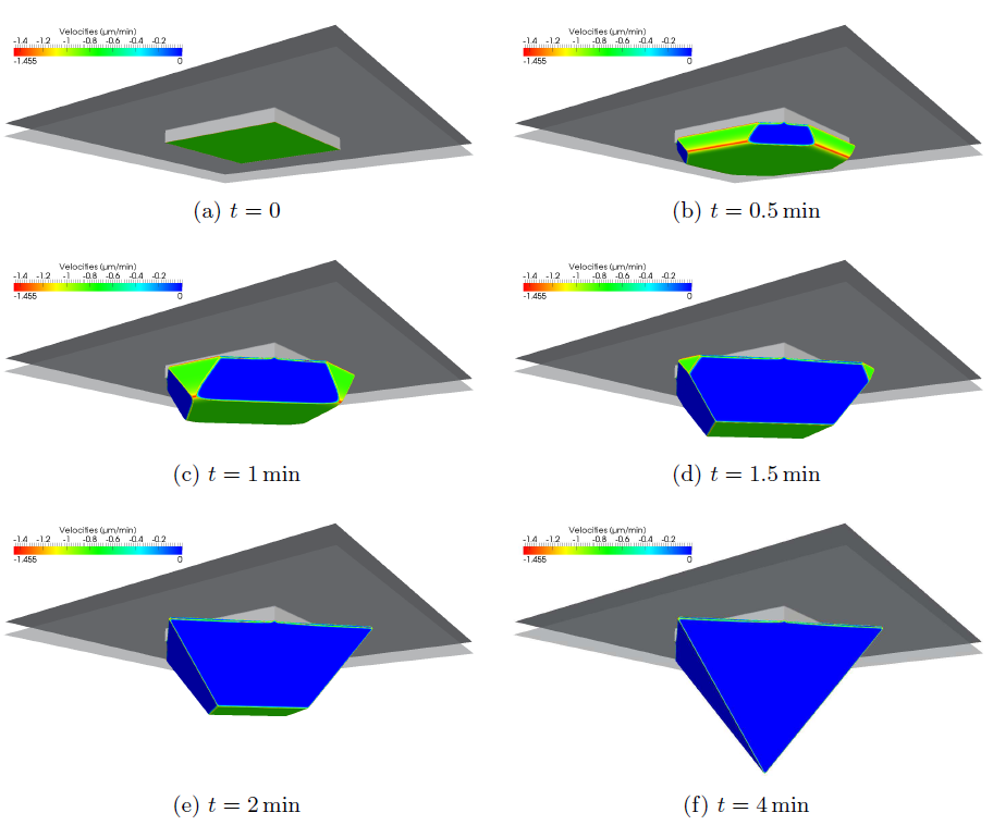
Some examples presented in [96] are reproduced by the following simulations. First, anisotropic wet etching of a silicon substrate through a mask with a quadratic hole is simulated. Due to the optimized LS framework, it is possible to use a very fine grid with a grid spacing of just
![]() . Since the extensions of the structure are
. Since the extensions of the structure are
![]() , the lateral grid extensions are
, the lateral grid extensions are
![]() . Two LS functions are used to represent the mask and the etch front. Figure 6.7 shows the LS representation at different times. The total calculation time was about
. Two LS functions are used to represent the mask and the etch front. Figure 6.7 shows the LS representation at different times. The total calculation time was about
![]() on two cores of an AMD Opteron 8222 SE processor (
on two cores of an AMD Opteron 8222 SE processor (
![]() ). If
). If
![]() is used for the CFL condition, approximately 3900 time steps are necessary. The total memory consumption did not exceed
is used for the CFL condition, approximately 3900 time steps are necessary. The total memory consumption did not exceed
![]() .
.
 |
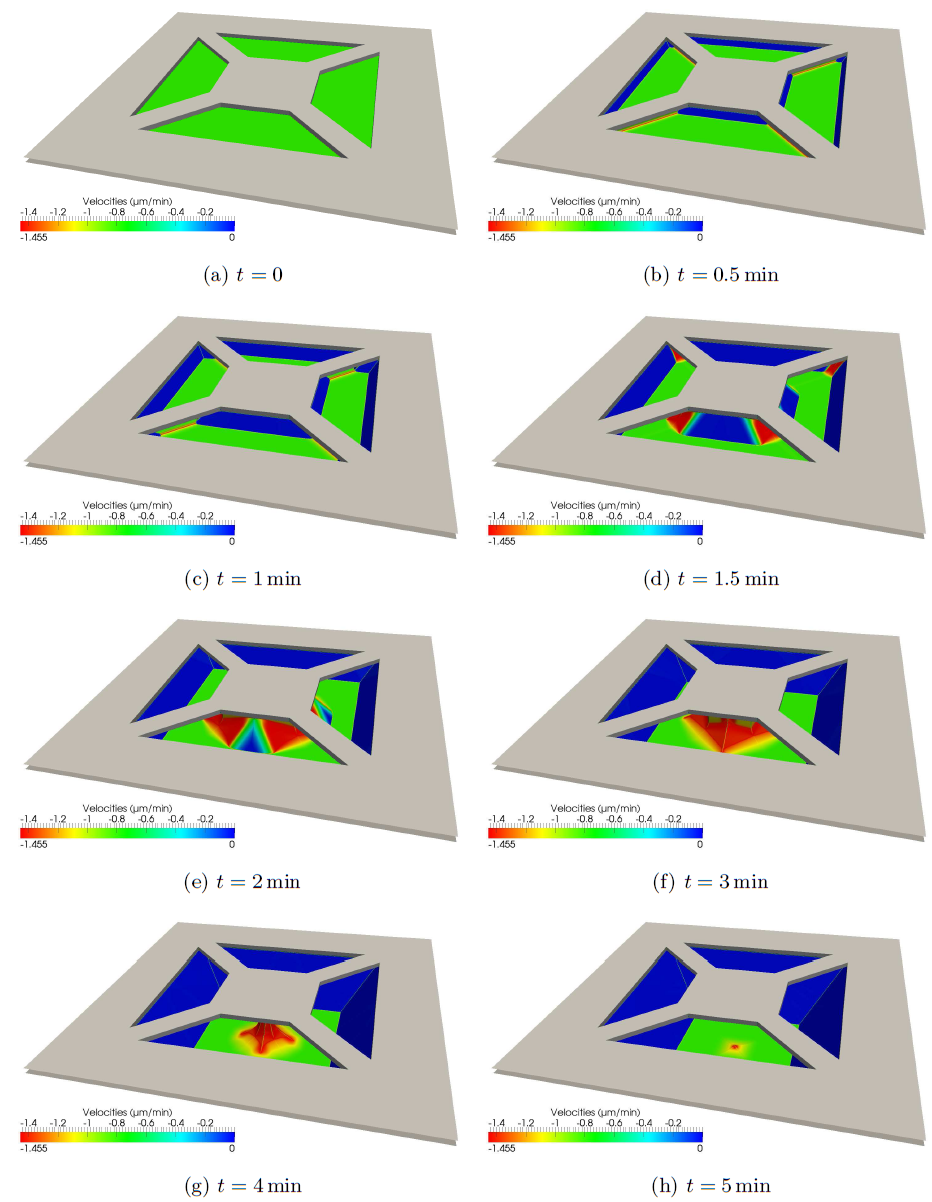
The results of a second simulation are shown Figure 6.8. There, a more complex mask structure is assumed with size
![]() . This leads to a grid with lateral extensions of
. This leads to a grid with lateral extensions of
![]() . Thanks to the H-RLE data structure, the total memory consumption was always below
. Thanks to the H-RLE data structure, the total memory consumption was always below
![]() . For comparison, the usage of a full grid with dimensions
. For comparison, the usage of a full grid with dimensions
![]() would require at least
would require at least
![]() for just storing the two LS functions. Using again
for just storing the two LS functions. Using again
![]() , the total calculation time for the required 12400 time steps was about
, the total calculation time for the required 12400 time steps was about
![]() on two cores of an AMD Opteron 8222 SE processor. The final profiles of both simulations are in good agreement with those reported in [96].
on two cores of an AMD Opteron 8222 SE processor. The final profiles of both simulations are in good agreement with those reported in [96].
 |