The impact of the field penetration into the gate on the flat-band potential,
threshold voltage, inversion-layer charge and  -
- characteristics of MOS
structure is analyzed in the following.
characteristics of MOS
structure is analyzed in the following.
For the sake of simplicity a uniformly doped bulk is assumed with concentration
 . For the
  relationship an expression analogous
with A.14 may be written. Relationships 2.2, 2.4, 2.6, 2.16 and the
relation form a closed implicit system of equations to determine
the field and potential in the structure at applied bias
relationship an expression analogous
with A.14 may be written. Relationships 2.2, 2.4, 2.6, 2.16 and the
relation form a closed implicit system of equations to determine
the field and potential in the structure at applied bias  . This system
is solved by a sequential method. The Newton iterative procedure is employed to
solve the field-potential equations with respect to potential. In the Newton
algorithm, limiting and damping are applied on the potential increments,
leading to a stable and fast convergency. This efficient technique has been
developed by the author in [162].
. This system
is solved by a sequential method. The Newton iterative procedure is employed to
solve the field-potential equations with respect to potential. In the Newton
algorithm, limiting and damping are applied on the potential increments,
leading to a stable and fast convergency. This efficient technique has been
developed by the author in [162].
For the reference device denoted as ``ideal'',  is assumed. Moreover,
 is adopted in the calculations.
Measurements have provided
is adopted in the calculations.
Measurements have provided  in
in  polysilicon and
 in
in  polysilicon [365]. Note that the
exact position of the Fermi level in degenerately doped polysilicon is
not well understood (see [275][200]). Regarding the data for the
electrical band-gap narrowing in single-crystal silicon, they are usually
extracted from the
polysilicon [365]. Note that the
exact position of the Fermi level in degenerately doped polysilicon is
not well understood (see [275][200]). Regarding the data for the
electrical band-gap narrowing in single-crystal silicon, they are usually
extracted from the  product in the quasi-neutral
regions, assuming a rigid-parabolic-band model. Using this data we are able to
reproduce the minority carrier concentration, but probably cannot accurately
determine the Fermi level position in heavily doped silicon and polysilicon.
product in the quasi-neutral
regions, assuming a rigid-parabolic-band model. Using this data we are able to
reproduce the minority carrier concentration, but probably cannot accurately
determine the Fermi level position in heavily doped silicon and polysilicon.
Flat-band potential
The flat-band potential loses its meaning for a nonhomogeneous structure like
the one considered here, because the flat-band condition cannot exist in the
whole structure in the general case. Hence we define the flat-band potential as
the gate-bulk bias corresponding to the flat-band condition in the bulk, which
we define by:
 ([95]). From
equations 2.4 and 2.6 it follows
([95]). From
equations 2.4 and 2.6 it follows
where  is the solution of the Poisson equation
in the bulk for vanishing surface field. Since we adopted a uniform bulk,
is the solution of the Poisson equation
in the bulk for vanishing surface field. Since we adopted a uniform bulk,
 holds. Two terms in expression 2.17
contribute to the
holds. Two terms in expression 2.17
contribute to the  -shift in implanted polysilicon-gate devices:
 ) and
) and
 , due to penetration of nonvanishing
electric field
, due to penetration of nonvanishing
electric field  into the gate.
 affects through the
term only. For a common value
affects through the
term only. For a common value
 [520] it follows
  from
equation 2.2. Assuming low-doped gate
from
equation 2.2. Assuming low-doped gate
 this field induces
  (accumulation
in
(accumulation
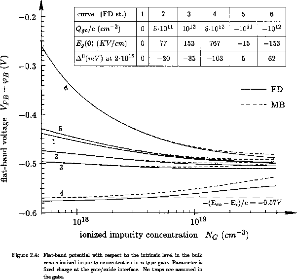
in  -type gate). Figure 2.4 shows the flat-band potential
with respect to intrinsic level in ideal silicon band
-type gate). Figure 2.4 shows the flat-band potential
with respect to intrinsic level in ideal silicon band  versus
the activated impurity concentration
versus
the activated impurity concentration  , with as
parameter. Showing instead of itself, the
characteristics become independent of the bulk doping. The calculations based
on both, Fermi-Dirac (FD) and Maxwell-Boltzmann (MB) statistics in the gate are
presented.
, with as
parameter. Showing instead of itself, the
characteristics become independent of the bulk doping. The calculations based
on both, Fermi-Dirac (FD) and Maxwell-Boltzmann (MB) statistics in the gate are
presented.
For positive the variation of with is nearly
logarithmic due to accumulation in the -type gate. has a weak
influence on . For a negative (not experimentally
detected [520]) the influence is stronger, because the gate becomes
depleted. Note that positive charges essentially ``improve''
, since the shift occurs towards the degenerate value. According to
the results shown in Figure 2.4, measurements of the flat-band
potential cannot serve as a reliable proof that a sufficiently high ionized
impurity concentration near the gate/oxide interface is achieved. For a
 -type gate positive may produce significant , because of
depletion in the gate. Assuming and
, as in the preceding example, we have
-type gate positive may produce significant , because of
depletion in the gate. Assuming and
, as in the preceding example, we have
 whereas
  leads to
 and a very large shift in . In the latter case,
although the bulk is holding at the flat-band, the onset of inversion takes
place in the gate, being produced exclusively by the charge at the gate/oxide
interface.
and a very large shift in . In the latter case,
although the bulk is holding at the flat-band, the onset of inversion takes
place in the gate, being produced exclusively by the charge at the gate/oxide
interface.
Measuring on MOS devices with different oxide thicknesses, the charge
at the oxide/bulk interface  (assuming vanishing
  ) may be
extracted from the linearly extrapolated
) may be
extracted from the linearly extrapolated  relationship [331][275][200][157]. This technique provides
the slope proportional to , but only the sum
relationship [331][275][200][157]. This technique provides
the slope proportional to , but only the sum  for
the intercept on the ordinate axis. Both factors, and
depend on the unknown activated impurity concentration near the gate/oxide
interface. Moreover, depends on too. Therefore, some
measurements in addition to measurements of are necessary to separate
(or
for
the intercept on the ordinate axis. Both factors, and
depend on the unknown activated impurity concentration near the gate/oxide
interface. Moreover, depends on too. Therefore, some
measurements in addition to measurements of are necessary to separate
(or  ) and . A second open question is how
defined by can be measured on MOS capacitors with nondegenerate gate
by, for example, some of the well established - techniques
([331]).
) and . A second open question is how
defined by can be measured on MOS capacitors with nondegenerate gate
by, for example, some of the well established - techniques
([331]).
In Figure 2.4 moderate doping has been considered.
is weakly affected by and close to its degenerate value
 . If the traps in the polysilicon are taken into account,
can vary significantly with decreasing doping levels due to trapping.
. If the traps in the polysilicon are taken into account,
can vary significantly with decreasing doping levels due to trapping.
Our calculations have clearly shown small differences between the results
obtained by Fermi-Dirac and Maxwell-Boltzmann statistics. The correction due to
degeneracy in determining the Fermi barrier is given by the second
term  in A.24. Assuming a gate doped
quite heavily
in A.24. Assuming a gate doped
quite heavily  this term increases by
only
this term increases by
only  and
and  for -type and -type gate, respectively at room
temperature (
for -type and -type gate, respectively at room
temperature ( ). Actually, the impact of FD statistics on our calculations
(carried out at room temperature) is smaller than the uncertainty in the
adopted model and the available experimental data for the band-gap narrowing.
For dopant concentrations higher than
). Actually, the impact of FD statistics on our calculations
(carried out at room temperature) is smaller than the uncertainty in the
adopted model and the available experimental data for the band-gap narrowing.
For dopant concentrations higher than  the differences
between FD and MB statistics become significant, but the polysilicon gates may
then be assumed to be degenerate.
the differences
between FD and MB statistics become significant, but the polysilicon gates may
then be assumed to be degenerate.
Threshold voltage
The threshold voltage is defined in the standard way as that  which
induces the minority surface concentration
which
induces the minority surface concentration  , for -type of bulk.
From relationships 2.4 and 2.6, it
follows
, for -type of bulk.
From relationships 2.4 and 2.6, it
follows
The upper index  denotes the values at the threshold. Remember that
 holds for bulk doped uniformly. The last five
terms at the right-hand-side in 2.18 are invariant with respect
to the effects in the gate. Two factors produce the deviation of the threshold
voltage of the nondegenerate-gate devices with respect to their degenerate-gate
counterparts:
holds for bulk doped uniformly. The last five
terms at the right-hand-side in 2.18 are invariant with respect
to the effects in the gate. Two factors produce the deviation of the threshold
voltage of the nondegenerate-gate devices with respect to their degenerate-gate
counterparts:
) and
 due to penetration of the electric field
into the gate.
due to penetration of the electric field
into the gate.
In thin-oxide devices the field
necessary to invert the oxide/bulk interface is very high due to the usually
high doping . For 2.19, a uniformly doped bulk is assumed.
Note that the bulk doping must be increased in thin oxide-devices, because the
contribution of the body-factor to the threshold voltage becomes smaller in
proportion with  . As a consequence of very high
  the surface
field in the gate is very high too and the surface potential
can be large.
the surface
field in the gate is very high too and the surface potential
can be large.
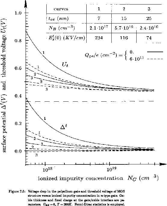
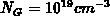
The results of the selfconsistent calculation at threshold are shown in
Figure 2.5.  and are given versus ,
with and being parameters. For different oxide thickness
the bulk doping is adapted so that the ideal threshold voltage
is the same for all devices (
and are given versus ,
with and being parameters. For different oxide thickness
the bulk doping is adapted so that the ideal threshold voltage
is the same for all devices ( , shown as dashed line in the
figure). The calculations show that both factors, and the deviations
of from the degenerate value are of the same order. The influence of
is considerably emphasized in thin-oxide devices (curve 1), because
of the high corresponding . For thick oxides the term becomes
quite small (curve 3). A positive charge at the gate/oxide interface
reduces the field (equation 2.2) and therefore, it
reduces . Assuming the values found in experiments [520]
for , this ``screening'' effect is rather pronounced. In
fact, a positive attenuates the increasing of due to
insufficient dopant concentration in -gate/-channel devices. An
eventual negative would have the opposite influence.
, shown as dashed line in the
figure). The calculations show that both factors, and the deviations
of from the degenerate value are of the same order. The influence of
is considerably emphasized in thin-oxide devices (curve 1), because
of the high corresponding . For thick oxides the term becomes
quite small (curve 3). A positive charge at the gate/oxide interface
reduces the field (equation 2.2) and therefore, it
reduces . Assuming the values found in experiments [520]
for , this ``screening'' effect is rather pronounced. In
fact, a positive attenuates the increasing of due to
insufficient dopant concentration in -gate/-channel devices. An
eventual negative would have the opposite influence.
Inversion-layer charge and capacitances
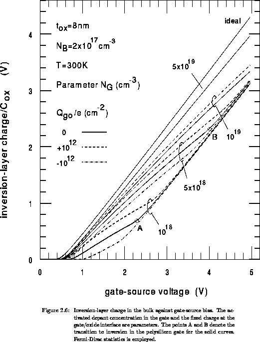
The surface field  is very high for strong inversion in thin-oxide devices,
even at medium gate bias. For example:
is very high for strong inversion in thin-oxide devices,
even at medium gate bias. For example:  on
on  result in
 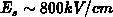 . Since the field is very high too, the
produced voltage drop in the gate
. Since the field is very high too, the
produced voltage drop in the gate  can significantly lower the effective
gate bias
can significantly lower the effective
gate bias  which is mostly responsible for the inversion-layer
charge
which is mostly responsible for the inversion-layer
charge  induced. As a consequence of a reduced the drain
current decreases, resulting in a degradation of the driving capabilities of
devices and the speed of the circuits. Figure 2.6 shows
plotted against with and as parameters.
is calculated by
induced. As a consequence of a reduced the drain
current decreases, resulting in a degradation of the driving capabilities of
devices and the speed of the circuits. Figure 2.6 shows
plotted against with and as parameters.
is calculated by
for uniformly doped bulk. As is well known,
formula 2.20 is very accurate (also in the
subthreshold region) [164][41]. The calculations are carried
out for a thin oxide of  which is typical for sub-
 CMOS technology. A pronounced reduction in is obtained even at high
 . Note that for the
differences of and from their degenerate counterparts are
quite small, Figures 2.4 and 2.5. A doping
higher than
. Note that for the
differences of and from their degenerate counterparts are
quite small, Figures 2.4 and 2.5. A doping
higher than  is necessary to obtain a negligible
voltage drop in the gate at the highest operating gate bias. The attenuation of
due to a screening is small for common values of . We may
judge to be the basic parameter which determines the degradation of
in strong inversion for a given .
is necessary to obtain a negligible
voltage drop in the gate at the highest operating gate bias. The attenuation of
due to a screening is small for common values of . We may
judge to be the basic parameter which determines the degradation of
in strong inversion for a given .
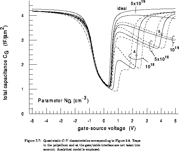
The quasi-static (QS) - characteristics, corresponding to
Figure 2.6, are given in Figure 2.7. The
total QS capacitance of the polysilicon-gate/oxide/silicon structure may be
defined by
where  and
and  are the total induced charge per unit area in bulk and
gate, respectively. may include the charge trapped at interface and
bulk traps in the polysilicon. Fixed charge in the oxide-volume
is considered as constant. Charge trapped at the gate/oxide and
oxide/bulk interfaces are included in and , respectively.
Differentiating expression 2.6 with respect to
one obtains
are the total induced charge per unit area in bulk and
gate, respectively. may include the charge trapped at interface and
bulk traps in the polysilicon. Fixed charge in the oxide-volume
is considered as constant. Charge trapped at the gate/oxide and
oxide/bulk interfaces are included in and , respectively.
Differentiating expression 2.6 with respect to
one obtains
The total capacitances per unit area of the polysilicon gate and the bulk are defined by
Expressions employed for  and
and  are collected in
Appendix A. Note that the interface traps are omitted in the
calculations shown in Figure 2.7. The ideal capacitance
follows from 2.22 for
are collected in
Appendix A. Note that the interface traps are omitted in the
calculations shown in Figure 2.7. The ideal capacitance
follows from 2.22 for  and the corresponding
selfconsistent .
and the corresponding
selfconsistent .
At a negative gate bias a small reduction in  occurs due to accumulation
in the gate. For positive effective gate voltages a significant lowering in
is caused by depletion in the gate. The decrease in depends
directly on and may be used as a figure of merit of the
degradation in and the drain current. A sharp recovery to the ideal
capacitance occurring for large positive voltages can be related to the
inversion in the gate near the gate/oxide interface (points A and B in the
figure). In Figure 2.6 the inversion in the gate is
manifested as a change in the slope of the
occurs due to accumulation
in the gate. For positive effective gate voltages a significant lowering in
is caused by depletion in the gate. The decrease in depends
directly on and may be used as a figure of merit of the
degradation in and the drain current. A sharp recovery to the ideal
capacitance occurring for large positive voltages can be related to the
inversion in the gate near the gate/oxide interface (points A and B in the
figure). In Figure 2.6 the inversion in the gate is
manifested as a change in the slope of the  characteristics. Even
for high the gate inversion occurs at a quite moderate gate bias in
thin-oxide devices. For example: at the point B we have
characteristics. Even
for high the gate inversion occurs at a quite moderate gate bias in
thin-oxide devices. For example: at the point B we have  ,
,
 ,
, 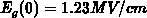 and
and  . Remark that for lower
the recovery of to the ideal value occurs at lower .
This finding is in qualitative agreement with the experimental characteristics
available in literature (Fig.1 in [281]).
. Remark that for lower
the recovery of to the ideal value occurs at lower .
This finding is in qualitative agreement with the experimental characteristics
available in literature (Fig.1 in [281]).
The same characteristics presented in Figures 2.5
and 2.6 are calculated employing MB statistics in the gate,
as well. The results, not shown here, differ only slightly from those obtained
by FD statistics. With respect to quantities in the bulk, like surface field
and inversion-layer charge, the influence of the degeneration due to Fermi-Dirac
statistics in the gate has no practical relevance at room temperature. With
regard to gate capacitance, small differences occur in the accumulation and at
the onset of gate inversion. Note that, although their impact on the total
capacitance is quite small, large differences between calculated
by FD and MB statistics occur in gate accumulation and inversion.
Some specific conclusions may be drawn from the calculations in this section:
and the charge at the gate/oxide interface
. The impact of on the flat-band potential and the
threshold voltage is found to be strong. Assuming a positive charge this
is particularly true for -gate/-channel devices.
due to gate depletion must be negligible
in the whole operating region. The activated concentration necessary
to meet this goal is considerably higher than the concentration
sufficient to obtain proper and , especially for
thin-oxide devices. Finally, we believe the measurements of both,
and are not proper indicators for the activated
impurity concentration in the gate close to the oxide. It is indispensible
to measure the complete quasi-static - characteristics in order to
evaluate the performance of implanted-gate MOSFETs.