In modern very large–scale integrated (VLSI) technologies complementary metal–oxide–semiconductor (CMOS) transistors face a broad range of operating, and hence, potential degradation regimes. For example, n– and p–channel FETs in a logic gate experience various \(\Vg \) and \(\Vd \) bias combinations during switching between logic levels. Assessing the reliability, on the other hand, typically focuses on idealized degradation modes, such as bias temperature instability (BTI), hot–carrier degradation (HCD) and time dependent dielectric breakdown (TDDB). Each of these reliability issues is usually evaluated in a certain bias space regime, see Fig. 1.1, and is experimentally and theoretically characterized around their respective worst–case stress condition. The individual degradation modes are, therefore, reasonably well understood and rather intricate models have been developed to capture the nature and characteristics of each phenomenon.
On the one hand, bias temperature instability and specifically the theoretical concepts behind this detrimental phenomenon, has gained much attention over the last decades [1]. Due to the aggressive downscaling of modern CMOS technologies together with the introduction of nitrogen into the oxide, the main research focus has been on the negative bias temperature instability (NBTI) in pMOSFETs. However, with the adoption of high–\(\kappa \) materials for the gate stack its counterpart, the positive bias temperature instability (PBTI), in nMOSFET transistors plays an equally important role nowadays. Despite the numerous research efforts BTI remains an active and controversial topic which is also reflected in the diversity of modeling approaches and their fundamentally diverging microscopic description.
In its early stages modeling approaches of BTI were based upon phenomenological observations which led to the model of Jeppson and Svensson in 1977 [2]. They assumed two different mechanisms within the low– and high–field regime to be responsible for the macroscopic shift of the threshold voltage: Breaking of interfacial Si–H bonds and the formation of mobile hydrogen or hydroxyl species and tunneling injection and trapping of holes activating surface states. This work provides the original formulation of the so–called Reaction–Diffusion model [1], which was able to explain the known power law dependence of the degradation, and served as a basis for further modifications until today. However, the introduction of new technology nodes using thin oxides together with advanced measurement setups such as time–dependent defect spectroscopy (TDDS) [3] revealed severe inconsistencies between the theoretical and experimental data [4]. Subsequently the research focus shifted towards the second mechanism which involves charge trapping into the oxide. The underlying physical process, however, has only been vaguely understood until Kirton and Uren in the 1990s described noise within the context of nonradiative multiphonon (NMP) theory of charge transitions [5]. Their pioneering work paved the way for further development by a broader community and was adopted by Grasser et al. to model the characteristics of BTI [6–11]. Within the recently published 4–state NMP model [6, 7, MJJ7] BTI, in particular its recoverable component, is attributed to charge trapping at pre–existing oxide defects in the gate stack. Thereby, it provides an accurate physical framework capturing even peculiar features such as defect metastability and has been successfully applied across various technologies [12–14, MJC11, MJC12, 15]. Despite the increasing acknowledgement of the NMP theory in the reliability community, soon after its development criticism was raised related to the role of the quasi permanent1 component of degradation and also the assumption that the 4–state formulation solely relies on pre–existing defects in the oxide. In response to these comments pursuing research efforts culminated in an evolution of the 4–state NMP framework in which the dynamic redistribution of hydrogen provides a link between the recoverable and quasi permanent component of degradation and further implements a possible defect creation mechanism [17–19]. Nevertheless, the heavily disputed field of bias temperature instability exhibits a continuously growing number of publications containing partially contradictory conclusions which renders it almost impossible for single a model to capture its various features and peculiarities.
On the other hand, hot–carrier degradation is attributed to a more permanent2 damage and is related to a different type of defect. It is widely accepted that Si–H bond rupture at or near the Si/SiO\(_2\) interface results in electrically active amphoteric traps. Over the past decades the phenomenon of HCD has evolved towards being the dominant and most troublesome reliability concern in modern technology nodes [20, 21]. Moreover, due to the continuous downscaling new challenges have emerged such as device–to–device variability and its implications on the reliability behavior has become a major issue. Random dopant variability and the generation of discrete random traps [22–25, MJJ5, 26, MJC7, MJC6] need to be taken into consideration as well as the effect of self–heating [27–30], which exacerbates the phenomenon of hot–carrier induced degradation in three–dimensional structures. All this serves to demonstrate the increasing complexity of modeling HCD to cover its broad physical spectrum. In that respect, modeling approaches have also advanced from phenomenological descriptions [31, 32] to more complex (semi–empirical) formulations [33–35, MJJ12] to capture the manifold phenomena contributing to HCD. However, while it is commonly accepted that hot–carrier damage is due to breaking of interfacial Si–H bonds resulting in electrically active Pb centers, its underlying fundamental physical mechanisms have not been fully clarified yet.
Hot–carrier degradation started to gain attention in the early 1970s with the first reports of this phenomenon [36]. Thereby, the term hot describes carriers in the channel which have been accelerated by the (high) electric field, particularly in the drain region of the metal–oxide–semiconductor field–effect transistor (MOSFET), and thus have gained a considerable amount of kinetic energy. Writing the energy as \(kT\) shows that the effective carrier temperature is many orders of magnitude higher than the surrounding lattice temperature. The first successful, although phenomenological, description of HCD characteristics was proposed by Hu et al. [31, 37]. The so–called Lucky Electron model originates from the work of Shockley [38] modeling the substrate and gate current and assumes that an energetic, lucky, electron impinges and surmounts the potential barrier at the interface thereby triggering the creation of a defect. Due to its simplicity it is still firmly entrenched in the community and several (semi–) empirical extensions have been suggested providing the foundations for the field–driven formulation of HCD [39–42]. Downscaling of transistor geometries below the micrometer regime together with the reduction of the operating voltages was expected to remedy hot–carrier related reliability issues. Yet, exactly the opposite has happened and HCD is highly relevant in scaled device architectures. In a series of experimental studies the IBM group investigated various stress regimes3 and concluded that the rate of interface state generation exclusively depends on the deposited energy by the carriers, independent of the stress mode [43–45]. These findings strongly inspired the development of the energy–driven paradigm of HCD by Rauch and LaRosa in which the driving force is the available carrier energy to trigger the creation of interface defects [33, 46]. The continued downscaling of CMOS technology further supported the idea that the carrier energy distribution function (EDF) becomes increasingly important and strongly depends on the bias conditions, which is also reflected in the change of the worst–case stress conditions from \(\Vg \sim 0.5\Vd \) to \(\Vg =\Vd \) for devices scaled into the nanometer regime. However, once again a next step in the evolution of HCD modeling was required for an advanced characterization and description of this phenomenon. The ground–breaking work by the group of Hess on the defect creation kinetics provides the cornerstone of modern modeling approaches and still defines the current understanding [47–52]. Acknowledging the crucial role of the EDFs, two individual degradation modes, known as the single carrier and multiple carrier mechanism, have been introduced accounting for the sparsely populated high energy tail as well as the part of the carrier ensemble having moderate energies. Unfortunately, the proposed formalism has never been applied to model the effect of HCD in an actual device. Nevertheless, the main concepts have been used by two groups, namely the group of Bravaix [34, 53–56] and Tyaginov [35, MJJ12, 57, MJC13, MJJ11, MJC18], and strongly influenced further developments4. Both modeling frameworks have successfully proven to capture the various trends of HCD across different technologies. However, technological innovations such as the introduction of FinFETs and nanowires in conjunction with new promising materials such as germanium constantly challenge the prevailing assumptions and demand a continuously improved and in–depth description of hot–carrier degradation [MJC13, MJC8, MJC9].
1 Note that the term quasi permanent components refers to the extremely slowly recovering contribution which sometimes is assumed to be permanent [16].
2 Although, also the damage created due to HCD can be annealed again.
3 Often stress regimes such as channel–, drain avalanche–, secondary generated and substrate hot–carrier stress can be found in the literature. In modern devices only channel hot–carrier stress is the relevant stress modes, which, however, includes the effects of drain avalanche and secondary generation of carriers.
4 These formulations are sometimes referred to as current–driven formulations
Reading the Introduction might suggest that the current modeling approaches already cover the full spectrum related to bias temperature instability and hot–carrier degradation, which would be a very abrupt end for this thesis. (Un–) Fortunately, a closer inspection reveals several open questions and missing links which initially triggered the research within this work and will hopefully be answered by the end.
Non–equilibrium carrier dynamics related reliability issues play the central role in this thesis. Charge carriers in the channel of a MOSFET are accelerated by the electric field and undergo various scattering mechanisms, thereby exchanging energy. This evolution results in a complex carrier energy distribution function (EDF), severely shifted from the equilibrium.
Carriers which have gained sufficient energy can trigger the creation of interface defects, known as HCD. Although the most recent stage of model developments relies on the concepts of a single and multiple carrier mechanism, their origin remains dubious and the fundamental excitation processes are not fully established yet. Furthermore, there is still no consensus on the actual microscopic Si–H bond–breaking kinetics and the associated potential barrier to form an electrically active interface trap. A major part of this thesis is devoted to the development of a general quantum kinetic formulation describing the dynamics of bond excitation and breaking mechanisms. All relevant system–bath interactions, such as vibrational relaxation and dipole scattering as well as resonance–induced excitations have been extracted using the close analogy to H terminated Si surfaces and the wealth of available experimental and theoretical studies. Ab initio methods performed on a realistic Si/SiO\(_2\) model have been applied to characterize the contribution of each individual mechanism and, furthermore, have been used to systematically address the question on how the H eventually dissociates away from the Si.
On the other hand, energetic carriers can penetrate into the oxide and get trapped at pre–existing oxide defects. However, the effect of charge trapping is usually evaluated within the BTI regime and hardly any studies have investigated the effect of non–equilibrium processes onto the (de–) trapping dynamics of oxide defects. Interestingly, also the 4–state NMP model is based on the equilibrium EDFs in order to evaluate the transition rates associated with charge capture and emission events. Therefore, an appealing and natural extension of the current BTI modeling framework towards full bias space explicitly includes non–equilibrium EDFs calculated as a solution of the Boltzmann transport equation (BTE). Additionally, a model variant with reduced complexity will be introduced which is particularly suited for modern technology computer–aided design (TCAD) applications.
This work not only aims at developing a better understanding of each individual degradation mode and the interaction of carriers with interface and oxide defects, but also gives new insights into the processes in full bias space. Overall, the presented results constitute a further step towards a Grand Unified Theory5 in the field of reliability, in which the two standard models for BTI and HCD are merged into a single framework.
5 This might sound familiar to a physicist.
reviews the state–of–the–art modeling frameworks for the creation of interface defects (HCD) and charge trapping at pre–existing oxide defects (BTI). Open questions and shortcomings of the current approaches are identified and the main ideas and concepts to address these open issues are introduced. Special attention is paid to the interaction of energetic charge carriers with individual chemical bonds. Several excitation mechanisms well known in the field of surface chemistry are highlighted and compared to the characteristics of HCD, which allows to derive the most important contributions given the conditions in a MOSFET: vibrational relaxation, dipole–induced as well as excitations due to a resonant scattering mechanism. Oxide defects, on the other hand, and the influence of non–equilibrium conditions onto the charging and discharging behaviour are considered as well. Possible extensions and approximations of the 4–state NMP model to calculate the phonon assisted transition rates are discussed: an extended model variant as well as a full non–equilibrium model using the calculated EDFs.
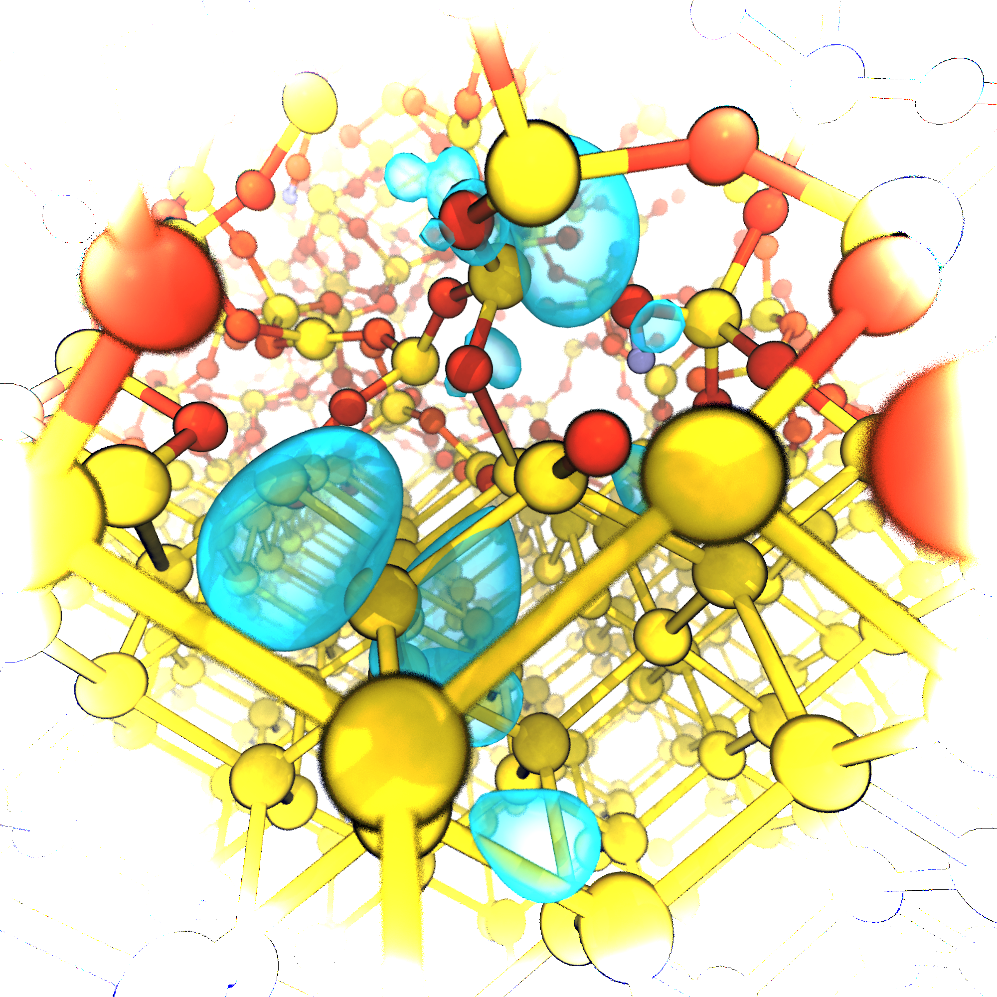
presents a detailed atomistic characterization of the Si–H bond and its properties using ab initio methods. First, the Si–H bond breaking trajectory will be revealed by means of different simulation methods using a classical force–field in conjunction with density functional theory (DFT). Furthermore, various properties of the Si–H complex and its environment are analyzed which are the key ingredients required by the theoretical concepts introduced before. Among them is the response to an applied electric field, the calculation of excited states and the vibrational coupling to its surrounding. In order to establish a complete picture of hydrogen related phenomena at the Si/SiO\(_2\) interface, H migration pathways along and across the interface as well as potential passivation reactions are examined at the end.
focuses on the theoretical formulations of the individual excitation and transitions rates. The dynamics of interface defects triggered by energetic charge carriers are described using open–system density–matrix theory. All relevant system–bath interactions are considered within this approach and the individual formulas are based on well established formulations in the literature. However, in contrast to existing theories, the modeling framework described here is coupled to a BTE solver to take the formation of non–equilibrium EDFs into account. Possible approximations to reduce the model complexity are discussed as well. Additionally, the theoretical foundations to describe the kinetics of oxide defects in full bias space will be established. Two variants of the 4–state NMP model with increasing levels of complexity will be presented. First, an extended model variant considering the electrostatics and the effect of impact ionization which, however, does not require information on the EDFs. Second, a full non–equilibrium 4–state model variant which explicitly relies on the coupled EDFs for electrons and holes.
summarizes the simulation results and compares them to experimental data. At the beginning both simulation approaches are individually tested in order to verify their capabilities. Comparing hot–carrier induced damage for an nMOSFET and a pMOSFET having different channel lengths at two temperatures reveals interesting degradation characteristics. The behaviour of oxide defects under non–equilibrium conditions, on the other hand, is examined using the measurements of single traps. Both developed modeling approaches are thoroughly tested and an in–depth analysis of the results further supports the corresponding findings. Subsequently, the presented work culminates in the modeling of a full {\(\Vg ,\Vd \)} bias map and a dedicated experiment with alternating stress conditions. Both results ultimately stress the conceptual limits of independent degradation modes.
briefly summarizes the key achievements of this thesis and highlights the most important findings. Furthermore, some suggestions and ideas for future improvements are listed.