The following Chapter provides an overview of the most advanced modern modeling approaches developed to capture the nature of bias temperature instability (BTI) and hot–carrier degradation (HCD). Shortcomings and open questions will be discussed and the key ideas to surmount the current limitations will be introduced.
Due to the in–depth description of both phenomena, the models are already based on the microscopic concept of potential energy surfaces (PESs). A PES describes the relation between the energy of a system and its geometry and is usually parametrized with respect to the position of the atoms. The Born–Oppenheimer approximation (BOA) is the cornerstone of modern computational chemistry and simplifies the full Schrödinger equation by separating it into an electronic and ionic part due to the mass disparity [58, 59]. This allows one to focus on the solution of the electronic wavefunction \(V(\mathbf {R})\) which acts as a potential for the ionic cores and includes Coulomb interactions as well as the contribution of the kinetic energy terms. For a system containing \(N\) atoms a PES is therefore a \(3N\)–dimensional object defining the energy as a function of the atomic coordinates. Modern ab initio codes offer a variety of functional forms with increasing complexity to evaluate the adiabatic potential. However, the large configuration space often prohibits the consideration of all degrees of freedom, particularly for transitions between different PESs involved in charge transfer reactions. Reducing a multi–dimensional PES \(V(\mathbf {R})\) to a one–dimensional potential energy curve (PEC) \(V(q)\) by selecting a reaction trajectory \(\mathbf {R}(q)\) and mapping the collective motion of atoms onto an effective reaction coordinate (RC) \(q\) is, therefore, desired for all practical applications. The reaction path ideally properly reflects the actual minimum energy path (MEP) connecting two minimum configurations with the lowest energy barrier. While for transitions within a single PEC this criterion is sufficiently fulfilled using a variant of the nudged elastic band (NEB) method, transitions across different PECs are determined by their crossing point and strongly depend on the chosen RC \(q\) and/or possible approximations schemes of the PEC, such as the harmonic approximation [8, MJJ7, 60–64]. Finding the minimum energy crossing point (MECP) of PECs for non–adiabatic charge transfer reactions is still a non–trivial optimization issue and an active research topic [65, 66]. Note that, regardless of the type of transition – within or across PEC(s) – the utilized MEP, hence the transition barrier, obeys classical mechanics.
The major breakthrough in modeling and understanding HCD in electronic devices is due to the work by the group of Hess [47–52]. This work serves as a basis for subsequent developments by two groups, namely the group of Bravaix [54, 56] and Tyaginov [35, MJJ12, MJC13, MJC19]. The main concept proposed by HESS is to link a thorough carrier transport treatment with two different but interacting regimes for defect creation.
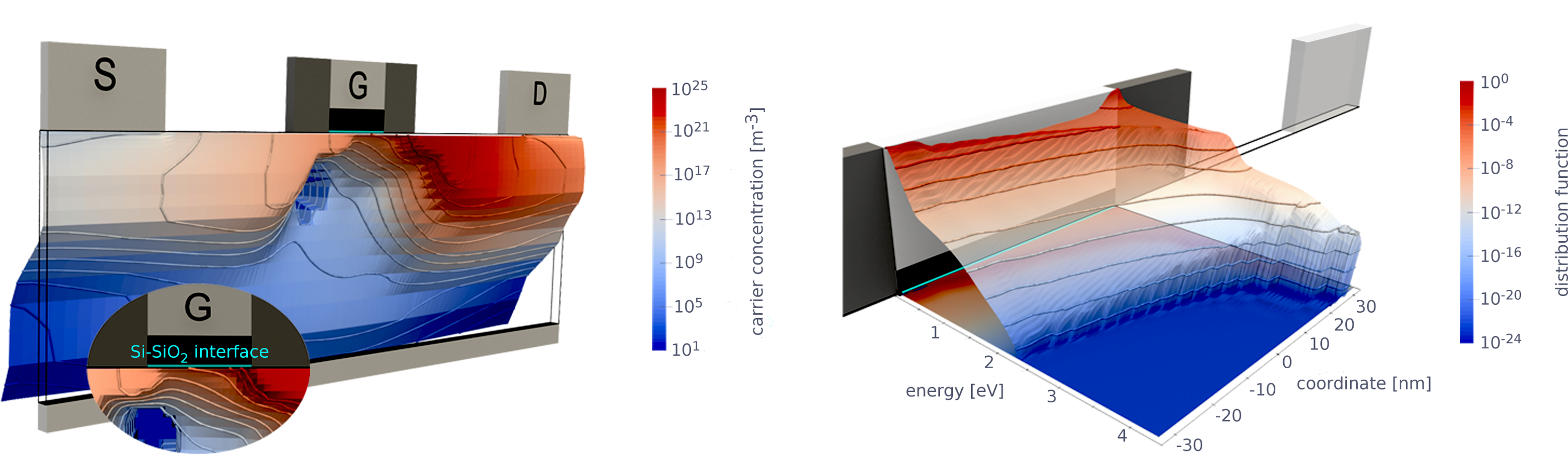
While carriers move through the channel of a MOSFET, they can undergo various scattering events. Scattering at ionized impurities, surface scattering as well as particle–particle, particle–phonon scattering and impact ionization facilitates energy exchange while particles are accelerated from source to drain by the electric field. This results in a broad and intricate distribution of energies including a high energy tail, i.e. heated carriers. The important quantity which, therefore, needs to be addressed is the carrier energy distribution function (EDF) [33–35, MJJ12, 48, 56, MJC17, MJJ10, 68], see Fig. 2.1, which provides information on how carriers are distributed over energy. Consequently, a solution of an appropriate (classical) transport equation, e.g. the Boltzmann transport equation (BTE), establishes the cornerstone of any microscopic HCD model.
Furthermore, according to Hess, the actual defect creation mechanism is governed by two modes, namely a single particle (SP) and a multiple particle (MP) mechanism. The SP process accounts for the high energy fraction of the carrier ensemble in the channel. Only one heated solitary carrier, with an energy greater than the threshold of this process, triggers direct desorption of hydrogen at the Si/SiO2 interface. Within its original formulation this interacting regime is based on the physical context of an electronic excitation of one of the bonding electrons. On the other hand, the MP mechanism describes a subsequent interaction of a multitude of carriers provoking a vibrational excitation of the Si–H bond. The authors of the original multi–carrier model of interface state generation [51] speculated about a resonance based process [52] as the underlying physical mechanism. Electrons potentially scatter into an accessible resonance state and thereby excite phonon modes of the Si–H system. However, this idea has never been implemented in an actual model. Modern approaches did not further pursue this concept and instead rely on empirical descriptions using a Keldysh like cross section of the MP mechanism [34, 35, 54], despite its importance in recent studies.
The most advanced model formulation developed by Tyaginov et al. assumes a harmonic potential energy profile for the Si–H bond with a dissociation energy of \(E_\mathrm {D}=\SI {2.56}{eV}\) and an energy spacing of the eigenlevels of \(\SI {0.25}{eV}\), which mimics the Si–H bonds stretching motion [MJJ12, MJC13]. However, no rigorous calculation of the Si–H bond breaking PES has been conducted so far, rendering the harmonic oscillator and its parameters an empirical approximation. The individual excitation rates between the eigenstates (MP) and direct dissociation (SP) are calculated using a formulation introduced by McMahon, the so–called acceleration integral [50, 51]. Initially derived from Fermi’s Golden Rule (FGR) to capture the interaction and scattering of an incident electron at the Si–H bond in order to explain the nonlinear dependence of HCD on the source–drain current using a multi–carrier process, it was later generalized towards the single carrier mode1. The acceleration integral represents the rate of excitation as the energy dependent carrier flux impinging the bond times a cross section
\(\seteqnumber{0}{2.}{0}\)\begin{equation} \Gamma _\mathrm {AB/SP}=\int f(E) g(E) v(E) \sigma (E-E_{\mathrm {th},i})^p \mathrm {d}E, \end{equation}
with \(f\) and \(g\) being the EDF and the density of states (DOS), \(v\) is carrier velocity and \(\sigma \) the cross section. Note that the term \(E_{\mathrm {th},i}\) in the cross section considers already excited phonon modes of the potential which reduces the effective barrier height and thus the threshold energy to trigger dissociation. Nevertheless, the energy dependence of the cross section, reflected by the exponent \(p\), is at best an empirically found relation. Despite its success, the model fails to fully and accurately describe the fundamental processes responsible for bond excitation.
The following Sections provide an overview of well known excitation mechanisms triggered by energetic carriers in the field of surface– and photochemistry. The close analogy to hot–carrier related reliability issues in electronic devices allows to establish the key concepts explaining the mechanisms leading to Si–H bond breakage at the Si/SiO2 interface. While dedicated experimental data sets are, however, only available within limited energy ranges, e.g. for scanning tunneling microscope (STM) induced Si–H bond breakage, it can be assumed that the same fundamental physical mechanisms are responsible for hot–carrier induced damage at the Si/SiO2 interface. The clear advantage of using deuterium over hydrogen to passivate a silicon dangling bond (DB), known as the giant isotope effect, has been found to be qualitatively the same for all studied systems, i.e. electronic devices [47, 69–73] and passivated surfaces [74–82]. Furthermore, the corresponding defect configurations, known as silicon dangling bonds (DBs), investigated on passivated Si surfaces are the same kind of defects also present in electronic devices, referred to as \(P_\mathrm {b}\) centers. The technologically relevant (100) Si/SiO2 interface exhibits two dominant types, the so–called \(P_\mathrm {b0}\) and \(P_\mathrm {b1}\) center. Both defects have been clearly identified using electron spin resonance (ESR) spectroscopy as a single \(sp^3\) hybrid facing a silicon atom vacancy with the (111) directions being a symmetry axes for \(P_\mathrm {b0}\), while the \(P_\mathrm {b1}\) defect possesses a lower symmetry [83–96]. This led to the conclusion that the \(P_\mathrm {b0}\) center is clearly associated with a trivalent interfacial Si back bonded to three Si atoms in the bulk. The properties of the \(P_\mathrm {b1}\) center, on the other hand, are quite controversial and different groups have suggested contradictory atomistic structures, ranging from a slightly distorted \(P_\mathrm {b0}\) center due to the amorphous Si/SiO\(_2\) interface to a silicon being bonded to two other silicons and an oxygen atom from the SiO\(_2\) [83, 84, 89, 91, 92, 97–99]. However, the overall characteristics of the \(P_\mathrm {b0}\) and \(P_\mathrm {b1}\) defect types at the Si/SiO\(_2\) interface render them compatible to DBs observed at passivated Si surfaces. This strongly indicates the similarities of the underlying processes, such as excitation and dissociation mechanisms.
1 Strictly speaking, the single particle (SP) process is physically prohibited due to the selection rules of a harmonic oscillator allowing only transitions of \(\Delta n+1\) or \(\Delta n-1\). However, an excited state as an intermediate step is assumed which effectively enables overtone transitions such as the SP mechanism.
Silicon and its properties are already well examined due to its extensive use as a semiconductor in solid–states devices and microelectronic applications. Controlling single adsorbates on surfaces has been proven to be a useful tool towards the understanding of individual reactions involving silicon [100]. Popular methods to modify surface patterns on the atomic scale, i.e. exciting and/or desorbing a single surface–adsorbate complex, include the scanning tunneling microscope (STM) and lasers, using either infrared or ultraviolet photons. While STM experiments use electrons to induce excitations, lasers can trigger adsorbate dynamics either directly or indirectly: In the direct case photons couple to the complex’s transition dipole moment, whereas the indirect route has been found to be substrate mediated [101]. Short pulses of light are able to excite a large number of electrons in the substrate which rapidly thermalize (due to the short electron–electron scattering length). The resulting hot electrons can interact with adsorbate resonances which eventually leads to dissociation [102, 103].
Reviewing the wealth of information available for Si–H bond breakage on passivated Si surfaces facilitates the separation of various excitation mechanisms and allows to extract the most important contributions. By comparing the requirements of individual processes to the conditions in a MOSFET, it is possible to link the well known DIET (desorption induced by electronic transitions) and DIMET (desorption induced by multiple electronic transitions) regimes to potential excitations in electronic devices. Note that, while the energetic situation in a MOSFET is certainly different compared to dedicated experiments using passivated surfaces, it can still be assumed that the physical principles of carrier interactions with solids, to be more specific, Si–H bonds, remain the same in both situations, see Fig. 2.2.

A significant contribution towards the understanding of STM induced Si–H bond breaking was made by the group of Avouris [78, 104, 105]. A major part of these studies is devoted to H dissociation triggered by electronic excitations. An excited electronic state of an adsorbate complex can be formed, for example, when one of the bonding electrons is excited to an (unoccupied) antibonding orbital. In order to cause such an electronic transition, the energy of the tunneling electrons emitted by the STM needs to exceed the threshold for this process, see Fig. 2.2 (1a). Provided that the newly created state is sufficiently repulsive, breaking of adsorbate–surface bonds can be induced. In the case of Si–H bonds this excitation channel is associated with a \(\sigma \Rightarrow \sigma ^*\) transition2, leading to a repulsive potential energy profile. Such a mechanism for Si–H bond breaking has been suggested in a series of papers [80–82, 106–113] with a threshold of \(\sim \SI {6.5}{eV}\) and a peak at \(\SI {8}{eV}\). Note that on a H terminated Si surface the release of a single atomic hydrogen is assumed to proceed via the Si–H stretching mode with a dissociation energy (into vacuum) of \(\sim \SI {3.6}{eV}\) [114, 115], see Fig. 2.2. Experimentally it was found that further increasing the energy of the STM electrons beyond \(\SI {8.5}{eV}\) did not impact the hydrogen desorption yield. Comparable results have been reported using laser light (\(\SI {157}{nm}\), \(\SI {7.9}{eV}\)) to provoke direct photodesorption of H from silicon surfaces with various orientations [116–118]. Both methods show an almost linear dependence of the dissociation yield \(Y\) with respect to the tunneling current \(I\) (or laser fluence \(F\)), \(Y\sim I\), which corresponds to the classic DIET regime. However, theoretical studies showed that an important competing effect of motion on the excited energy profile is the so–called electronic quenching [74, 104], which will relax the system back to its ground state. Due to the very short lifetime of the excited state (in the order of femtoseconds), this efficient mechanism results in hydrogen desorption originating from a rather hot ground state instead of the excited potential.
2 \(\sigma \): occupied bonding orbital, \(\sigma ^*\): unoccupied antibonding orbital
Reducing the sample bias of the STM below the threshold of the electronic excitation, results in a lower, but non–zero H desorption yield [106, 114, 119]. Within the energy range of the incident electrons between \(\SI {2}{}\) and \(\SI {6}{eV}\) the yield \(Y\) strongly depends on the applied voltage and the tunneling current [114, 115, 119–121]. This corresponds to the characteristics of the DIMET regime, where \(Y\sim I^n,\,(n>1)\) with \(n\) being approximately the number of electrons needed to trigger dissociation. The underlying mechanism is due to tunneling electrons resonantly scattering at an adsorbate state, see Fig. 2.2 (2c), thereby exciting vibrational modes of the ground state potential [104, 114, 119]. Such a resonance state and the corresponding scattering process on solid state systems and surfaces is defined in close analogy to its gas phase counterpart [112, 122]. Essentially, it is an electron–impact phenomenon where the impinging carrier triggers the formation of a transient atomic or molecular ion. Thereby, the incident electron (or hole) is temporarily captured in the vicinity of the molecule in a (quasi–) bound molecular orbital, typically an antibonding orbital, forming a short–lived negative (positive) ion resonance state. The trapped electron (hole) will be re–emitted again after \(10^{-10}\) to \(10^{-15}\,\mathrm {s}\), which is the typical lifetime of a resonance. Such a process is manifest as a characteristic peak or resonance in the incoming carrier energy as well as the scattering cross section, hence it is commonly referred to as resonance carrier scattering or resonance excitation.
In the case of the Si–H bond it is assumed that the anionic resonance (a scattering state for an electron) is associated with the unoccupied \(\sigma ^*\) orbital, whereas the cation resonance state for energetic holes is formed by the occupied \(\sigma \) orbital [114, 115, 119]. Qualitatively similar results, albeit on different adsorbate–substrate combinations, have been obtained using optically excited hot substrate electrons scattering into an available resonance [101–103, 123, 124]. This, however, shows the universal applicability and validity of resonance mediated excitations.
Although the measurement data reported by various groups [104, 106, 114, 119] could be explained quite well by different vibrational heating models, using either a coherent or an incoherent formulation, the details of the mechanism are not fully understood yet. Both models assume that an electron attaches to an unoccupied orbital, thus forming a negative ion resonance. Upon inelastic electronic relaxation, it transfers a part of its energy to the bond’s vibrations. While in the incoherent formulation only one quantum of energy can be transferred, the coherent model allows the electron to excite a larger number of vibrational quanta within the bonding potential. However, in more recent publications [119, 125] it was shown that fewer electrons are needed to dissociate hydrogen than assumed in the incoherent model3. The conclusions drawn by the authors render the coherent formulation to be more compatible to the observed behaviour.
3 In which the number of electrons equals the number of bound states in the potential.
Another important excitation mechanism is related to the interaction of the vibrational transition dipole of an adsorbate with an electric field. The electric field caused by the electrons which tunnel from the STM tip to the surface is able to couple to the bond’s dipole moment and induce transitions between vibrational states. However, his mechanism usually requires a rather high current density between the tip and the sample. On the other hand, for a large current of energetic, hot, carriers, the resonance scattering process described above typically dominates the excitation dynamics and, thus, renders dipole induced excitations of only minor importance.
Based on the detailed picture of the various excitation processes together with the understanding of how charge carriers can interact with an adsorbate complex, the fundamental framework to describe hot–carrier related degradation phenomena in MOSFETs can be derived. There is an unambiguous connection between experimentally observed Si–H bond breaking processes induced by dedicated measurement techniques, Fig. 2.2 (1) and (2), and HCD in electronic devices, see Fig. 2.2 (3). One possibility is clearly associated with an electronic excitation, namely the \(\sigma \Rightarrow \sigma ^*\) transition. However, rather high energetic carriers of about \(\SI {6}{}-\SI {8}{eV}\) are needed to trigger such a mechanism, which renders it incompatible to carrier energies typically observed in MOSFETs. On the other hand, a combination of resonance scattering and vibrational heating seems more likely to be the driving force for the creation of defect states at the Si/SiO\(_2\) interface. The moderate carrier energies required for this excitation channel together with its strong current dependence agree well with the characteristic features of hot–carrier effects in MOSFETs. Dipole–induced vibrational excitations are more complicated to quantify. Contrary to STM experiments, where tunneling currents are injected from the tip and the Si–H bond is assumed to be perpendicular to the surface4, the conditions at the Si/SiO\(_2\) interface are not that well defined. Charge carriers move parallel to the interface in the inversion layer of the MOSFET with additional spatial varying electric fields being present during operation. Furthermore, the Si–H bond direction is not necessarily perpendicular to the Si/SiO\(_2\) interface and its dipole moment is not aligned with the field direction.
4 This is true for a H:Si(111) surface and partly fulfilled for a H:Si(100)-(2\(\times \)1) surface where the top layer is dimerized due to the surface reconstruction.