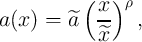
-Based Memristors
-Based MemristorsAccording to Eq. 3.7, the term  for the TiO
 -based memristor is obtained as
 | (6.11) |
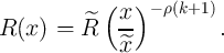
From Eq. 3.8, we then obtain
 | (6.12) |
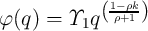
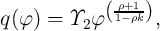
Therefore, we get
 | (6.13) |
Thus, according to Eq. 6.4 and Eq. 6.5, this device can be used for charge-based memristive sensing.
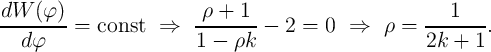
Let us consider a memristor-capacitor (MC) circuit shown in the inset of Fig. 6.5d. Fig. 6.5a
shows the  characteristics of the memristor, when the MC circuit is excited by a step
voltage source
characteristics of the memristor, when the MC circuit is excited by a step
voltage source  where
where  =0 for
  and 1 for
  . The memristor exhibits
different behavior for different capacitances. As it is expected, the smaller the capacitance the
smaller the charging time (Fig. 6.5b) as well as the smaller the charge modulation. Thus, the
memristance exhibits smaller modulation for smaller capacitance (Fig. 6.5c). This is the key idea to
measure the capacitance by using Eq. 6.4 based on the modulations of the voltage across the
capacitor and the memristance. According to Eq. 6.4, if the measurement is performed after the
capacitor is fully charged (
. The memristor exhibits
different behavior for different capacitances. As it is expected, the smaller the capacitance the
smaller the charging time (Fig. 6.5b) as well as the smaller the charge modulation. Thus, the
memristance exhibits smaller modulation for smaller capacitance (Fig. 6.5c). This is the key idea to
measure the capacitance by using Eq. 6.4 based on the modulations of the voltage across the
capacitor and the memristance. According to Eq. 6.4, if the measurement is performed after the
capacitor is fully charged ( ), only the memristance modulation has to be measured.
However, depending on the readout resolution, the measurement can be performed in a time interval
(much) shorter than the full charge time (Fig. 6.5d). In Fig. 6.5, the TiO
), only the memristance modulation has to be measured.
However, depending on the readout resolution, the measurement can be performed in a time interval
(much) shorter than the full charge time (Fig. 6.5d). In Fig. 6.5, the TiO -based memristor
device characteristics are assumed as
-based memristor
device characteristics are assumed as  ,
,  ,
,  , and
, and
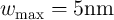 [69].
[69].
| Figure 6.5.: | (a) TiO memristor memristor  curves. (b) The voltage of the capacitor and (c) the memristance as a function
of time. (d) Obtained capacitances by using Eq. 6.4. curves. (b) The voltage of the capacitor and (c) the memristance as a function
of time. (d) Obtained capacitances by using Eq. 6.4. |
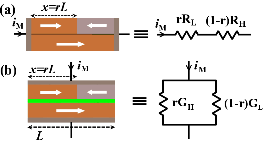
Fig. 6.6 shows two magnetoresistive spintronic memristors with current-induced domain wall motion in a
giant magnetoresistance spin-valve (Fig. 6.6a) and a tunneling device (Fig. 6.6b). The electrical resistance
(conductance) of these devices  (
( ) is a function of the DW position (
 ) in the magnetic
free layer [96, 94, 137]. A complete antiparallel alignment results in a high-resistance state (HRS;
) in the magnetic
free layer [96, 94, 137]. A complete antiparallel alignment results in a high-resistance state (HRS;
 ) of the device, while a fully parallel alignment places it in a low-resistance state (LRS;
 ).
).
For the domain wall giant magnetoresistance (DW-GMR) the memristor  is given by [96]
R(r) =  | = RP(r) + RAP(r) = rRL + (1 - r)RH | ||
| = RH - r(RH - RL) = (1 - rGMR)RL, | (6.14) |
where  is the domain wall position,
  represent the relative DW position, and
  denotes the
length of the free layer.
denotes the
length of the free layer.  is the giant magnetoresistance ratio. According to Eq. 4.4,
the electrical conductance of the domain wall tunnel magnetoresistance (DW-TMR) memristor is obtained
as [137]
is the giant magnetoresistance ratio. According to Eq. 4.4,
the electrical conductance of the domain wall tunnel magnetoresistance (DW-TMR) memristor is obtained
as [137]
G(r) =  | = GP(r) + GAP(r) = rGH + (1 - r)GL | ||
| = (1 + rTMR)GL | (6.15) |
 is the tunneling magnetoresistance ratio. The term
  (
( ) is obtained
from Eq. 6.16 (Eq. 6.17) for the DW-GMR (DW-TMR) memristors, where
) is obtained
from Eq. 6.16 (Eq. 6.17) for the DW-GMR (DW-TMR) memristors, where  is the DW
velocity.
is the DW
velocity.
 | (6.16) |
 | (6.17) |
According to Eq. 6.16 (Eq. 6.17), in the DW-GMR (DW-TMR) memristor the term  (
( ) is a constant and thus is suited for charge- (flux)-based measurement, if there is a linear
relationship between the domain wall velocity (
) is a constant and thus is suited for charge- (flux)-based measurement, if there is a linear
relationship between the domain wall velocity ( ) and the current
  (voltage
  ). It
can be shown that a linear dependence of the DW velocity with respect to the applied current
or voltage is expected, when the ratio
). It
can be shown that a linear dependence of the DW velocity with respect to the applied current
or voltage is expected, when the ratio  is nonzero, where
  is the damping parameter
and
is the damping parameter
and  defines the strength of the non-adiabatic spin-torque [174, 175]. In fact, for
  the
DW exhibits a threshold current density required for current-induced motion, even when in the
absence of an extrinsic pinning [170, 176]. Thus, only in the presence of non-adiabatic spin-torque
(
the
DW exhibits a threshold current density required for current-induced motion, even when in the
absence of an extrinsic pinning [170, 176]. Thus, only in the presence of non-adiabatic spin-torque
( ), the DW-GMR and the DW-TMR memristors can be used for charge- and flux-based
sensing. In fact, the non-adiabatic spin-torque allows for a non-zero mobility of the DW where the
mobility is proportional to the ratio
), the DW-GMR and the DW-TMR memristors can be used for charge- and flux-based
sensing. In fact, the non-adiabatic spin-torque allows for a non-zero mobility of the DW where the
mobility is proportional to the ratio  [210, 211]. A comprehensive interpretation of the
non-adiabatic spin-torque expressed by
[210, 211]. A comprehensive interpretation of the
non-adiabatic spin-torque expressed by  is still subject to controversial discussions and there are
also difficulties to experimentally characterize
is still subject to controversial discussions and there are
also difficulties to experimentally characterize  [174, 212, 213, 214]. In [213] experimental
data shows
[174, 212, 213, 214]. In [213] experimental
data shows  ratios of
  and
and  for CoNi multilayers and FePt alloy thin films,
respectively.
for CoNi multilayers and FePt alloy thin films,
respectively.
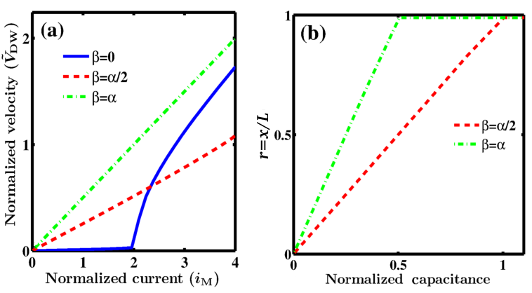
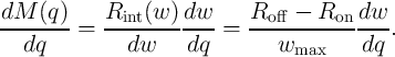
| Figure 6.7.: | (a) Average domain wall velocity as a function of  . (b) Final relative domain wall position ( . (b) Final relative domain wall position ( ) as a
function of capacitance. ) as a
function of capacitance. |
As an example of a spintronic capacitance sensor, Fig. 6.7a shows the average DW velocity as a function of
the current passing through the DW-GMR memristor (connected in series to a capacitor as shown in
Fig. 6.1a) based on the one-dimensional model of DW dynamics explained in Section 4.2.2. According to
Eq. 6.16, the memristor is suited for capacitance sensing when  . Fig. 6.7b illustrates that when the
MC circuit (Fig. 6.1a) is excited by a step voltage the final domain wall position in the DW-GMR memristor
and thus the memristance value is a function of the capacitance value. The sensitivity increases with
the ratio
. Fig. 6.7b illustrates that when the
MC circuit (Fig. 6.1a) is excited by a step voltage the final domain wall position in the DW-GMR memristor
and thus the memristance value is a function of the capacitance value. The sensitivity increases with
the ratio  , but at the cost of decreased sensing range. In fact, the increase in the ratio
 , increases the DW velocity and thus the sensitivity. It should be noted that for
  , the
DW propagation is characterized by a linear regime and a nonlinear regime above the Walker
breakdown [215, 174, 216]. Above a critical current value called the Walker breakdown, the DW motion
becomes non-uniform (oscillatory) which is unfavorable for memristive sensing as discussed in the
following.
, the
DW propagation is characterized by a linear regime and a nonlinear regime above the Walker
breakdown [215, 174, 216]. Above a critical current value called the Walker breakdown, the DW motion
becomes non-uniform (oscillatory) which is unfavorable for memristive sensing as discussed in the
following.
The dynamic properties of a propagating magnetic DW are strongly affected by the device geometry [217]. A
magnetic thin-film (MTF) element with varying width  and constant thickness
  (Fig. 6.8a) has been
proposed as a spintronic (DW-MTF) memristor [61] based upon the STT-induced DW motion in the
film-length direction
(Fig. 6.8a) has been
proposed as a spintronic (DW-MTF) memristor [61] based upon the STT-induced DW motion in the
film-length direction  . The reaction force exerted by the domain wall to the electrons acts as the wall
resistance [61]. The current-induced DW motion exhibits memristive properties, when the thin-film aspect
ratio
. The reaction force exerted by the domain wall to the electrons acts as the wall
resistance [61]. The current-induced DW motion exhibits memristive properties, when the thin-film aspect
ratio  is varying with
  . Indeed, when the thickness of the device is fixed, the mobility of the DW
and thus the electrical resistance of the device, becomes a function of the thin-film element width
. Indeed, when the thickness of the device is fixed, the mobility of the DW
and thus the electrical resistance of the device, becomes a function of the thin-film element width  and
is expressed as [61]
and
is expressed as [61]
 | (6.18) |
where  and
and  are the resistance and the width of the element, respectively, when the DW is located at
 and
and  determines the DW mobility scaling with the aspect ratio as
  [61]. Therefore,
when the spatial dependence of the element width as a function of the DW position is given
by
[61]. Therefore,
when the spatial dependence of the element width as a function of the DW position is given
by
 | (6.19) |
the  characteristics of the device is obtained as
 | (6.20) |
where we have [61]
 | (6.21) |
Since the dynamics of the magnetic domain wall motion ( ) is a function of
  and current density
(
and current density
( ), the latter equation shows that this device is a memristive system (Eq. 2.14 and Eq. 2.15). For
an idealistic case in which the DW velocity is proportional to the current density, the
), the latter equation shows that this device is a memristive system (Eq. 2.14 and Eq. 2.15). For
an idealistic case in which the DW velocity is proportional to the current density, the  and
and  constitutive relations of the domain wall magnetic thin-film (DW-MTF) memristor are determined
as [61]
constitutive relations of the domain wall magnetic thin-film (DW-MTF) memristor are determined
as [61]
 | (6.22) |
and
 | (6.23) |
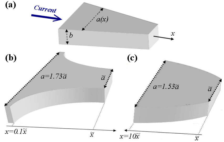
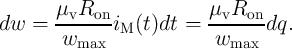
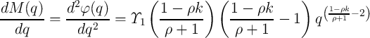
| Figure 6.8.: | (a) Domain wall magnetic thin-film (DW-MTF) spintronic memristor with appropriate geometries for (b) charge-based and (c) flux-based sensing. |
where  and
and  are constant coefficients and
  determines the spatial dependence of the element’s width
on
determines the spatial dependence of the element’s width
on  (Eq. 6.19) [61, 172]. According to Eq. 2.10 (Eq. 2.11) and Eq. 6.22 (Eq. 6.23), for charge
(flux)-controlled DW-MTF memristor we obtain
(Eq. 6.19) [61, 172]. According to Eq. 2.10 (Eq. 2.11) and Eq. 6.22 (Eq. 6.23), for charge
(flux)-controlled DW-MTF memristor we obtain
 | (6.24) |
and
 | (6.25) |
Therefore, in order to keep the terms  and
and  fixed, the appropriate device geometries for
charge- and flux-based memristive sensing methods are (uniquely) determined by
fixed, the appropriate device geometries for
charge- and flux-based memristive sensing methods are (uniquely) determined by
 | (6.26) |
and
 | (6.27) |
In fact, different device geometries can provide different memristive behaviors required for various sensing
applications. With a spatial shape of  (
( ), the DW-MTF memristor is suited
for charge (flux)-based sensing. Fig. 6.8 shows schematic geometries for memristive sensing where the
parameter
), the DW-MTF memristor is suited
for charge (flux)-based sensing. Fig. 6.8 shows schematic geometries for memristive sensing where the
parameter  is supposed equal to
  [172].
| Figure 6.9.: | (a) DW-MTF memristor  curves. (b) The current flowing through the inductor and (c) the memductance
as a function of time. (d) The electric circuit for flux-based inductance sensing and the obtained inductances by using
Eq. 6.9. curves. (b) The current flowing through the inductor and (c) the memductance
as a function of time. (d) The electric circuit for flux-based inductance sensing and the obtained inductances by using
Eq. 6.9. |
Fig. 6.9 shows an example of inductance sensing by using the DW-MTF memristor with proper geometry
based on Eq. 6.9. The applied current is 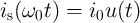 and all axes are dimensionless, with current,
memductance, voltage, time, and angular frequency normalized in units of
and all axes are dimensionless, with current,
memductance, voltage, time, and angular frequency normalized in units of  ,
,  ,
,  ,
,  ,
and
,
and  .
.  is the memductance when the domain wall position is
  and
and  is equal to
 . According to Fig. 6.9a, the memristor shows different memristive behavior for different
inductances connected in parallel. Therefore, by using Eq. 6.9 (Fig. 6.9d), the amount of inductance
can be calculated when the current (Fig. 6.9b) and memductance (Fig. 6.9c) modulations are
known.
. According to Fig. 6.9a, the memristor shows different memristive behavior for different
inductances connected in parallel. Therefore, by using Eq. 6.9 (Fig. 6.9d), the amount of inductance
can be calculated when the current (Fig. 6.9b) and memductance (Fig. 6.9c) modulations are
known.
| Figure 6.10.: | (a) Time-varying capacitance and memristive measurement results. (b) The domain wall position and (c)
the source voltage  and the voltage across the capacitor and the voltage across the capacitor  and (d) the current flowing through the memristor and (d) the current flowing through the memristor  with respect to time.
 |
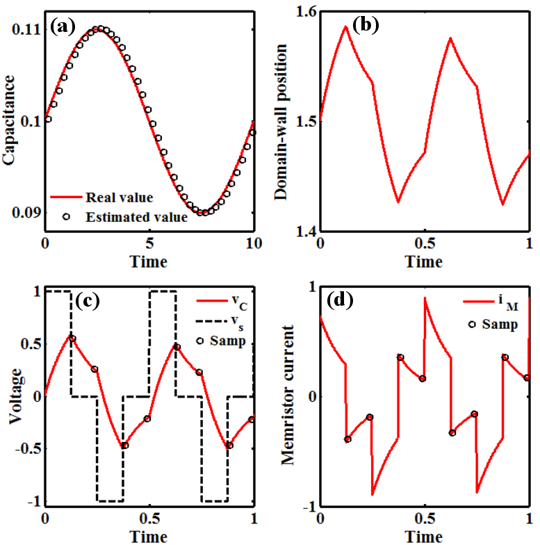
| Figure 6.11.: | (a) Time-varying inductance and memristive measurement results. (b) The domain wall position and (c)
the source current  and the current flowing through the inductor and the current flowing through the inductor  and (d) the voltage of the memristor and (d) the voltage of the memristor  with
respect to time. with
respect to time. |
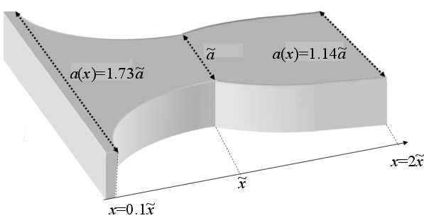
| Figure 6.12.: | Proposed DW-MTF memristor structure for simultaneous capacitance and inductance sensing. |
Fig. 6.10 and Fig. 6.11 show the simulation results for memristive measurement of time-varying capacitors
and inductors. The voltage  and current
  sources are pulse trains with a 50% duty cycle and a
magnitude of
sources are pulse trains with a 50% duty cycle and a
magnitude of  and
and  and the capacitance and inductance are normalized by
  and
and  ,
respectively.
,
respectively.  (
( ) is equal to
  (
( ), where
  (
( ) corresponds to the memristance
(memductance) when domain wall is located at
) corresponds to the memristance
(memductance) when domain wall is located at  . By sampling
  and
and  the capacitance
(inductance) can be calculated using Eq. 6.4 (Eq. 6.9). Fig. 6.12 shows a DW-MTF memristor
structure suited for both capacitance and inductance sensing. The term
the capacitance
(inductance) can be calculated using Eq. 6.4 (Eq. 6.9). Fig. 6.12 shows a DW-MTF memristor
structure suited for both capacitance and inductance sensing. The term  (
( ) is
constant for
) is
constant for  (
( ) and the corresponding memristance and memductance are shown in
Fig. 6.13.
) and the corresponding memristance and memductance are shown in
Fig. 6.13.
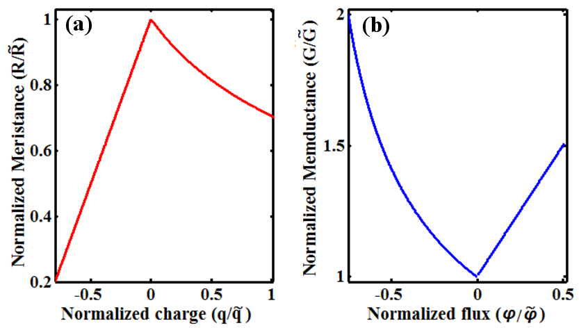
| Figure 6.13.: | (a)  as a function of charge and (b) as a function of charge and (b)  as a function of flux for the DW-MTF memristor structure
shown in Fig. 6.12. as a function of flux for the DW-MTF memristor structure
shown in Fig. 6.12. |
In order to take a closer look at the DW dynamics in a patterned structure, the one-dimensional
model of DW dynamics (Section 4.2.2) is employed to analyze the DW-MTF-based memristive
sensing. The dynamic properties of a propagating magnetic DW are strongly affected by the device
geometry [217]. The varying width of the DW-MTF element (Fig. 6.12) is taken into account by
assuming the current density and the number of spins ( ) in the DW [170] as a
function of the DW position
) in the DW [170] as a
function of the DW position  . Therefore, Eq. 4.8 is solved for
  and
and
 .
.
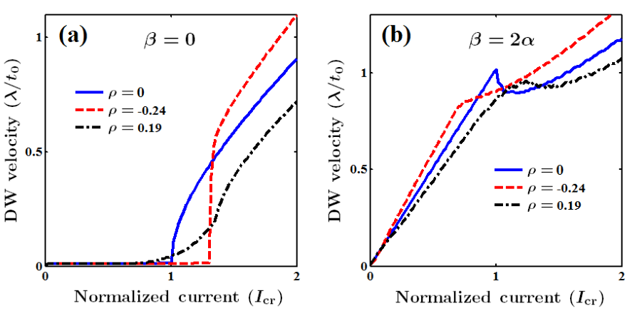
| Figure 6.14.: | Time-averaged domain wall velocity (a) in the absence and (b) in the presence of the non-adiabatic
spin-torque effect plotted for different geometrical structures ( ). ). |
Fig. 6.14 shows the geometry dependence of the DW dynamics for zero and nonzero non-adiabatic
spin-torque values. In the absence of the non-adiabatic term (Fig. 6.14a), there is a geometry dependent
threshold current required to move a DW. Therefore, for the currents below a current threshold the
memristive behavior can not be observed. In the presence of the non-adiabatic term (Fig. 6.14b), the average
DW velocity increases linearly with the applied current for low current values. Therefore, with
 , the memristive behavior is observed and with proper geometry, the device can be used for
memristive sensing. Above a (geometry dependent) critical current corresponding to the Walker
breakdown [215, 174, 216], the DW motion shows complex behaviors. Therefore, the memristive sensing has
to be performed in a low current regime, which for a given sensing resolution, increases the sensing
time.
, the memristive behavior is observed and with proper geometry, the device can be used for
memristive sensing. Above a (geometry dependent) critical current corresponding to the Walker
breakdown [215, 174, 216], the DW motion shows complex behaviors. Therefore, the memristive sensing has
to be performed in a low current regime, which for a given sensing resolution, increases the sensing
time.