Chapter 8
Numerical Results
In the previous chapters comparisons for the proposed methods have mostly been given for a
 -diode. The aim of this chapter is to show that the proposed methods blend well and lead
to considerable performance improvements for realistic device geometries. First, spatially
two-dimensional simulations are presented for a MOSFET-like device. Then, it is shown that the
combination of the proposed extensions to the SHE method allow for the simulation of a fully
three-dimensional FinFET on an average workstation.
-diode. The aim of this chapter is to show that the proposed methods blend well and lead
to considerable performance improvements for realistic device geometries. First, spatially
two-dimensional simulations are presented for a MOSFET-like device. Then, it is shown that the
combination of the proposed extensions to the SHE method allow for the simulation of a fully
three-dimensional FinFET on an average workstation.
The average workstation is considered to be a machine equipped with a Intel Core i7 960
CPU, 12 GB RAM and a NVIDIA GeForce GTX 580. For simplicity, Dirichlet boundary
conditions are used at the contacts and a parabolic energy band model is employed.
Self-consistency of the Poisson equation, the SHE equations for electrons, and the drift-diffusion
equation for holes is obtained by means of a damped Gummel iteration. The energy spacing is set
to  meV, and acoustical, optical and ionized impurity scattering mechanisms are considered.
For simplicity, doping profiles are chosen constant in each segment of the device. Note that doping
profiles in realistic devices are smeared out due to unavoidable diffusion, which is beneficial for
the numerical stability. Since the more challenging case of constant doping profiles
is considered here, the results in this chapter can be transferred to realistic doping
profiles.
meV, and acoustical, optical and ionized impurity scattering mechanisms are considered.
For simplicity, doping profiles are chosen constant in each segment of the device. Note that doping
profiles in realistic devices are smeared out due to unavoidable diffusion, which is beneficial for
the numerical stability. Since the more challenging case of constant doping profiles
is considered here, the results in this chapter can be transferred to realistic doping
profiles.
The meshes used in the next sections are generated with Netgen [91]. Simulator output is
written to VTK files [59], which are then processed for visualization by the open-source software
ParaView [58].
8.1 MOSFET
The adaptive variable-order scheme presented in Chap. 6 is applied to the simulation of an
 -channel MOSFET in unipolar approximation with a channel length of
  nm. Simulations
are carried out using the unstructured triangular mesh depicted in Fig. 5.7. The doping
concentration in the source and drain regions are set to
nm. Simulations
are carried out using the unstructured triangular mesh depicted in Fig. 5.7. The doping
concentration in the source and drain regions are set to  cm
cm , and to
  cm
cm in the channel and in the bulk regions. A high-k hafnium oxide with a thickness of
 nm is used. Doping profiles change abruptly between the individual regions for
simplicity. Note that this is not realistic from a technological point of view, and is
usually more challenging for the numerical point of view. The source and the bulk
contacts are grounded, while the drain contact is biased at
nm is used. Doping profiles change abruptly between the individual regions for
simplicity. Note that this is not realistic from a technological point of view, and is
usually more challenging for the numerical point of view. The source and the bulk
contacts are grounded, while the drain contact is biased at  Volts. The gate voltage is
set to
Volts. The gate voltage is
set to  Volts. Due to the unipolar approximation with rather high doping in the
channel region, there is a spurious current flow between the drain and the body contact.
Nevertheless, the characteristic behavior in the channel is observed and is used for an
evaluation.
Volts. Due to the unipolar approximation with rather high doping in the
channel region, there is a spurious current flow between the drain and the body contact.
Nevertheless, the characteristic behavior in the channel is observed and is used for an
evaluation.
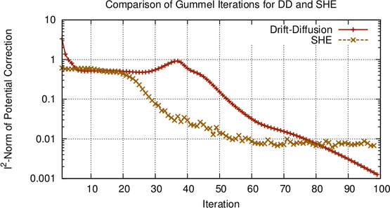
To obtain self-consistency with the Poisson equation, a damped Gummel iteration of a
first-order SHE with  iterations and a damping coefficient of
  is carried out. The discrete
 -norm of the potential update vector in each iteration is depicted in Fig. 8.1. Comparable
convergence behavior is obtained for both the drift-diffusion and the SHE approach. Note that
the SHE simulation starts with a lower, yet significant initial update, because the result of
the drift-diffusion simulation is used as initial guess for the SHE simulation. As the
iteration progresses, the SHE method saturates, which stems from the discretization
error with respect to the potential-dependent band edge influencing the simulation
domain in
-norm of the potential update vector in each iteration is depicted in Fig. 8.1. Comparable
convergence behavior is obtained for both the drift-diffusion and the SHE approach. Note that
the SHE simulation starts with a lower, yet significant initial update, because the result of
the drift-diffusion simulation is used as initial guess for the SHE simulation. As the
iteration progresses, the SHE method saturates, which stems from the discretization
error with respect to the potential-dependent band edge influencing the simulation
domain in  -space, cf. Sec. 2.3. In any case, the potential update is essentially
homogeneous over the device, hence the infinity norm of the potential update is around
-space, cf. Sec. 2.3. In any case, the potential update is essentially
homogeneous over the device, hence the infinity norm of the potential update is around
 .
.
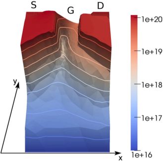
Simulated carrier concentrations are depicted in Fig. 8.2. Densities have been computed from
a uniform fifth-order SHE, while Gummel iterations for self-consistency have been
carried out for a first-order SHE only. The inconsistencies near the source and drain
contacts are due to the lack of full self-consistency of the fifth-order SHE with the Poisson
equation, which is amplified by the use of Dirichlet boundary conditions. Consequently, it
is concluded that it is insufficient to ensure self-consistency with a first-order SHE
only.
Inside the channel a pinch-off can readily be observed. Furthermore, the plot of the carrier
density above one electron Volt shows the exponential increase of carriers with high energy along
the channel. It has to be emphasized that such an information cannot be obtained from
macroscopic transport models such as the drift-diffusion model. For the unipolar simulation of a
MOSFET considered here, a high population of heated electrons is obtained all over
the drain region, which is about ten orders of magnitude higher than in the source
region.
Fig. 8.3 shows a plot of the electrostatic potential and the energy distribution function. Due
to the small device dimensions, carriers are injected quasi-ballistically into the drain region. This
leads to high values of the distribution function at kinetic energies around  eV, which is the
cause of the high concentration of electrons above 1 eV shown in Fig. 8.2. Furthermore, the
Dirichlet boundary conditions at the drain contact lead to a boundary layer of the
distribution function, which is a purely numerical effect. Therefore, other boundary
conditions such as those proposed by Hong et al. [42] should be used for predictive device
simulation.
eV, which is the
cause of the high concentration of electrons above 1 eV shown in Fig. 8.2. Furthermore, the
Dirichlet boundary conditions at the drain contact lead to a boundary layer of the
distribution function, which is a purely numerical effect. Therefore, other boundary
conditions such as those proposed by Hong et al. [42] should be used for predictive device
simulation.
Figure 8.4: Error indicator and expansion order distribution after the first and second
adaption step. At the contacts, the error indicator is set to  and a first-order expansion
is preserved. Here, the bulk is kept at a fixed first order, since the contribution to transport
is negligible. The vertical axis denotes total energy.
and a first-order expansion
is preserved. Here, the bulk is kept at a fixed first order, since the contribution to transport
is negligible. The vertical axis denotes total energy.
The decay-based strategy as discussed in Chap. 6 is applied for an adaptive variable-order
SHE using the same parameters as for the simulation of the  diode to the
MOSFET. Clearly, the obtained results are not the best possible, yet they allow for
judging the need for parameter adjustments over a wider range of devices. Fig. 8.4
shows the expansion order indicators obtained from a uniform first-order SHE and
from the subsequent variable-order simulation. The expansion orders after the first and
the second adaption step are particularly increased near the band-edge and around
the channel. In the drain region, a hot energy tail of the distribution function leads
to an increase of the expansion order above
diode to the
MOSFET. Clearly, the obtained results are not the best possible, yet they allow for
judging the need for parameter adjustments over a wider range of devices. Fig. 8.4
shows the expansion order indicators obtained from a uniform first-order SHE and
from the subsequent variable-order simulation. The expansion orders after the first and
the second adaption step are particularly increased near the band-edge and around
the channel. In the drain region, a hot energy tail of the distribution function leads
to an increase of the expansion order above  eV only. At very high energies, a
first-order expansion is preserved. It is worthwhile to note that almost all third-order
expansion nodes become fifth-order expansion nodes after the second adaption step.
Additional savings from a better parametrized error indicator are therefore expected.
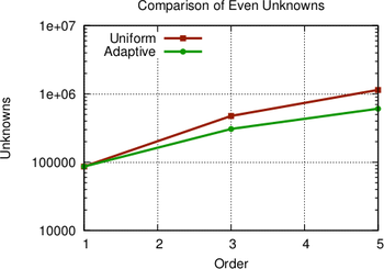
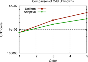
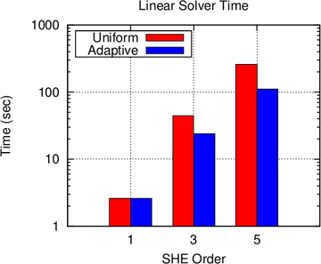
Nevertheless, the number of unknowns in Fig. 8.5 is reduced by a factor of up to two for
fifth-order expansions, and execution times are reduced by a factor of almost five due to
the sparser population of the system matrix at lower expansion orders, cf. Fig. 8.6.
The high gain in execution time may also be due to better caching possibilities on the
CPU, because data operations are more localized and thus less cache misses occur.
Performance gains from a parallelization are comparable to the results in Sec. 7.4.
It has to be mentioned that a uniform fifth-order SHE of the MOSFET leads to a
linear system and a preconditioner which is too large in order to fit into GPU RAM.
Therefore, additional fallback-mechanisms are required when using GPU acceleration with
SHE.
eV only. At very high energies, a
first-order expansion is preserved. It is worthwhile to note that almost all third-order
expansion nodes become fifth-order expansion nodes after the second adaption step.
Additional savings from a better parametrized error indicator are therefore expected.
Nevertheless, the number of unknowns in Fig. 8.5 is reduced by a factor of up to two for
fifth-order expansions, and execution times are reduced by a factor of almost five due to
the sparser population of the system matrix at lower expansion orders, cf. Fig. 8.6.
The high gain in execution time may also be due to better caching possibilities on the
CPU, because data operations are more localized and thus less cache misses occur.
Performance gains from a parallelization are comparable to the results in Sec. 7.4.
It has to be mentioned that a uniform fifth-order SHE of the MOSFET leads to a
linear system and a preconditioner which is too large in order to fit into GPU RAM.
Therefore, additional fallback-mechanisms are required when using GPU acceleration with
SHE.
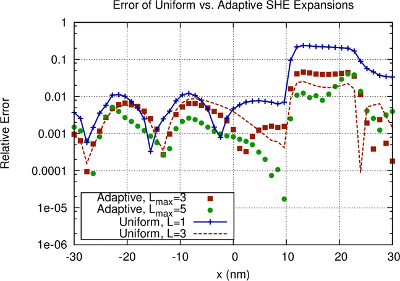
A comparison of the average carrier energy in Fig. 8.7 again confirms convergence of the SHE
method and further shows that adaptive expansion orders lead to accuracy comparable to
uniform expansions. The kinks in the error function are due to the interpolation of
the solution quantities along a line passing through the mesh at a depth of  nm
below the gate oxide. It is crucial to note that unlike in the case of the
nm
below the gate oxide. It is crucial to note that unlike in the case of the  diode
simulated in Sec. 6.3, a first-order SHE leads to a significant error in the average carrier
energy, thus confirming that higher-order SHE is indeed required for modern scaled-down
devices.
diode
simulated in Sec. 6.3, a first-order SHE leads to a significant error in the average carrier
energy, thus confirming that higher-order SHE is indeed required for modern scaled-down
devices.
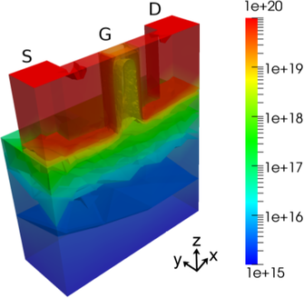
8.2 FinFET
While transistors have been fabricated as planar devices over decades, the small feature sizes of
modern devices leads to the undesired effect that the gate loses control over the current flow. One
of the possible remedies currently employed is the use of fully three-dimensional device layouts,
such that the channel is fabricated as a fin, and the gate is wrapped around the fin in order to
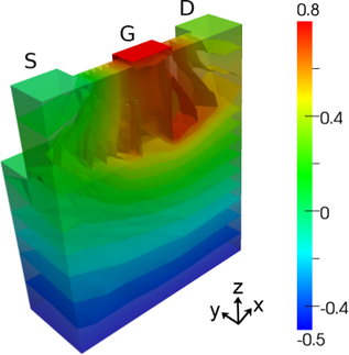
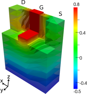
have better control over the current flow. A schematic view of such a so-called FinFET is
given in Fig. 8.8 and investigated in the following. Since three faces of the channel
are used to control current flow, the device is sometimes also referred to as trigate
transistor.
Due to symmetry considerations along the fin, it is sufficient to simulate only one half of the
device. The simulated device has a channel length of  nm and the mesh used for the
simulation is depicted in Fig. 5.8. A constant doping of
nm and the mesh used for the
simulation is depicted in Fig. 5.8. A constant doping of  cm
cm is applied in the source
and drain contacts, while a doping of
is applied in the source
and drain contacts, while a doping of  cm
cm is applied in the channel and in
the bulk. Again, the device is simulated in an unipolar approximation. The source
contact is grounded, the drain contact is biased by
is applied in the channel and in
the bulk. Again, the device is simulated in an unipolar approximation. The source
contact is grounded, the drain contact is biased by  Volt, a gate voltage of
  Volt is applied, and the bulk contact is grounded. Due to the difference in the built-in
potential, the Dirichlet boundary conditions for the potential at the bulk contact are set
to
Volt is applied, and the bulk contact is grounded. Due to the difference in the built-in
potential, the Dirichlet boundary conditions for the potential at the bulk contact are set
to  Volt. The results presented in the following are obtained from a uniform
first-order SHE, and at the end of this section an adaptive SHE up to third order is
discussed.
Volt. The results presented in the following are obtained from a uniform
first-order SHE, and at the end of this section an adaptive SHE up to third order is
discussed.
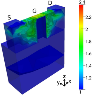
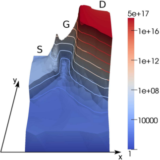
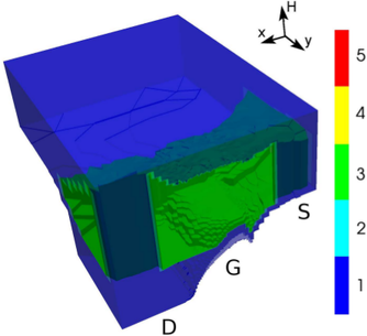
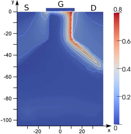
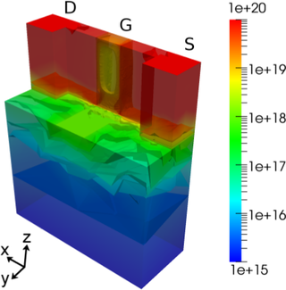
Fig. 8.9 shows the carrier density inside the device. The accumulation of carriers near the gate
oxide is clearly visible, especially along the oxide on top. In the center of the channel, a region of
lower carrier density is obtained.
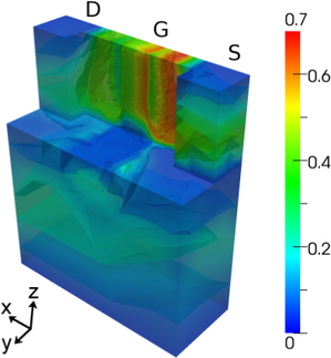
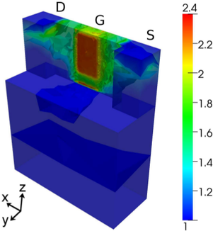
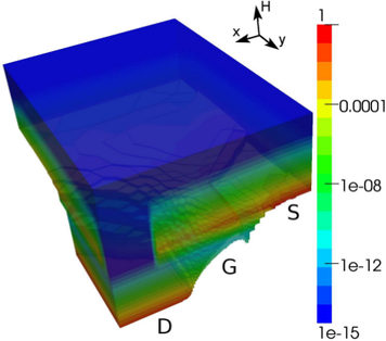
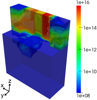
The density of carriers above  eV shown in Fig. 8.10 shows a high concentration of hot
carriers in the source and drain region towards the channel. The peak concentration is obtained at
the beginning of the gate oxide in the source region.
eV shown in Fig. 8.10 shows a high concentration of hot
carriers in the source and drain region towards the channel. The peak concentration is obtained at
the beginning of the gate oxide in the source region.
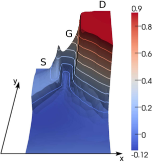
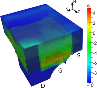
The potential distribution inside the device is depicted in Fig. 8.11, which also depicts the
potential inside the oxide. Note that the oxide also extends towards the bulk, where three times
the thickness around the fin is chosen. However, the oxide grown on the bulk does not contribute
to carrier transport significantly.
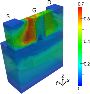
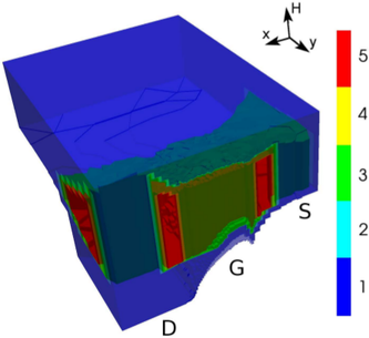
Average carrier energies are shown in Fig. 8.12. In contrast to the MOSFET with a high
drain-source bias, the low drain-source bias for the FinFET leads to high average carrier energies
mostly in the source close to the gate oxide. The elevated carrier energies deeper in the source are
due to the high bulk bias.
While the uniform first-order SHE has lead to  even-order unknowns leading to a
memory consumption of
even-order unknowns leading to a
memory consumption of  GB, a uniform third-order expansion results in
  even-order
unknowns and a memory consumption beyond
even-order
unknowns and a memory consumption beyond  GB. Since this is beyond the memory
provided by the workstation, only an adaptive SHE up to third-order is carried out. Using
the same adaptive strategy based on the rate of decay of the expansion coefficients
as for the MOSFET,
GB. Since this is beyond the memory
provided by the workstation, only an adaptive SHE up to third-order is carried out. Using
the same adaptive strategy based on the rate of decay of the expansion coefficients
as for the MOSFET,  even-order unknowns are obtained, which is still too
large for the workstation. Reducing the threshold value from
even-order unknowns are obtained, which is still too
large for the workstation. Reducing the threshold value from  to
to  and
clamping the bulk and the interior of the channel to first-order results in
and
clamping the bulk and the interior of the channel to first-order results in  unknowns, which just fits into the
  GB budget. The expansion order averaged over
the full energy range is depicted in Fig. 8.13. The adaptive strategy readily resolves
the crucial regions underneath the gate oxide, even though a rather high threshold is
chosen.
GB budget. The expansion order averaged over
the full energy range is depicted in Fig. 8.13. The adaptive strategy readily resolves
the crucial regions underneath the gate oxide, even though a rather high threshold is
chosen.


 of
the distribution function.
of
the distribution function.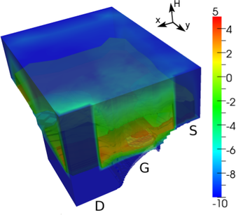
 for a
third-order expansion, and a factor of
for a
third-order expansion, and a factor of  for a fifth-order expansion.
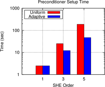
 nm below
the gate oxide, with
nm below
the gate oxide, with  corresponding to the center of the channel. The convergence
of the SHE method can readily be seen and adaptive expansions essentially agree with
corresponding uniform expansions.
corresponding to the center of the channel. The convergence
of the SHE method can readily be seen and adaptive expansions essentially agree with
corresponding uniform expansions.
 ) in the simulated FinFET. The color scale is
truncated below
) in the simulated FinFET. The color scale is
truncated below  cm
cm in order to have a higher resultion in the channel.
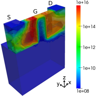
 eV (in cm
 ) in the simulated
FinFET.
) in the simulated
FinFET.