

3 Anisotropic Wet Etching
Since the beginning of semiconductor device fabrication, anisotropic wet etching has been an essential processing technique [89]. This particular type of etching plays an important role in the field of MEMS due to its reliability and simplicity [9] and is still applied for specific applications in microelectronics, e.g., wet etching of sapphire. The anisotropic etch rates can be modeled in a similar way to SEG. During both processes crystal facets with well-defined crystallographic orientations emerge. Some concepts introduced in the previous section can be transferred to anisotropic wet etching. Nevertheless, in this chapter the fundamentals of anisotropic wet etching are introduced and several approaches to modeling the 3D etch profiles are discussed.
3.1 Fundamentals of Anisotropic Wet Etching
In semiconductor micro-fabrication there are two forms of material removal techniques: dry and wet etching. Dry etching proceeds in an etch chamber with a gaseous atmosphere. There is a variety of physical and chemical
mechanisms which can be employed to achieve controlled removal of thin films. A rough classification involves reactive (plasma etching, RIE) and non-reactive etching (sputter etching, ion beam etching). The etching mechanism
can either be isotropic (same etch rate in every direction) or anisotropic. The former category of processes tends to produce isotropic profiles, while the latter results in more pronounced anisotropy. Fig. 3.1 illustrates the impact of (an)isotropy on the resulting etch profile in a typical mask configuration. Wet etching is based on liquid-phase chemicals (etchants) which
remove specific materials by gradually decomposing the surface and dissolving the reaction products. In order to subject a substrate to wet etching, the wafer is immersed in appropriate wet etching chemistry. Isotropic wet etching
of  is possible with HNA (hydrofluoric, nitric, acetic) solutions. The widely used wet etchant potassium hydroxide (
  ) has the property of etching with very high anisotropy. In particular, characteristic surfaces (e.g.,
  ) emerge during etching. Since these surfaces are intrinsic crystal facets of , the etch profile is well predictable and can be used fabricate specific geometric features, such as mask undercut or V-shaped profiles.
In this section, the microscopic reasons for highly anisotropic wet etching are addressed first before several anisotropic etchants for various materials and their properties and characterization are discussed.


3.1.1 Microscopic Processes During Anisotropic Wet Etching
There are some wet etchants which remove material isotropically and some which have pronounced anisotropy. Isotropic etching processes are typically transport-controlled [90]. Hereby, the chemical etch rate is determined by the rate of transport of the etchant to the substrate. The reaction takes place on a time scale significantly shorter than the transport. Therefore, properties of the surface and bulk material to etch do not affect etch rates and thus etching proceeds isotropically. In contrast, anisotropic etching proceeds in the surface reaction-limited regime. Reactants are sufficiently fast transported to the surface and microscopic surface reactions determine the net etch rate [91].
The details of surface reactions associated with anisotropic wet etchants are complex. Typically, reactions consist of several stages and multiple intermediate reaction products. Ultimately, the final products need to be soluble in
order to be transported away from the surface. Nevertheless, simplified models have been proposed to understand why certain crystal surfaces are etched with substantially higher rates than others [92], [93]. These models are mostly focusing on wet etching of and provide an adequate picture of the underlying mechanisms. In the following, the essentials of these models are outlined.

A surface of a crystalline material is characterized by the specific arrangement of its atoms. Fig. 3.2 illustrates a segment of the surface, showing steps and
terraces. Depending on the local neighborhood and whether an atom resides on a step or terrace, the atomic bonds have a characteristic configuration. In a wet etching process, surface atoms are removed from the crystal. Hence,
surface and volume bonds have to be freed during the chemical etch reaction. In order to describe the etch reaction, the crystal surface can be considered as being composed of idealized atom types which reflect arrangement, bonds,
and hydrogen saturation. Examples for these idealized atoms are step monohydride, terrace monohydride, step dihydride, or terrace trihydride (Fig. 3.2). Here,
the prefix (mono, di) expresses the number of non- - bonds, which are typically saturated with hydrogen [94]. Surfaces with different crystal orientation,
have different characteristic arrangements of these idealized atoms.
A fundamental observation is that the relative etch rates of different planes depend on a chemical and a geometrical component. The chemical component can be described based on the idealized atoms. For instance, terrace monohydride atoms are unlikely to be removed, because breaking of three volume bonds is required. The general tendency is: The higher the number of surface bonds, the higher the etch rate. In order to etch a plane, a multi-step process takes place and generally involves the removal of multiple atom types [93], [95]. The removal rate is also affected by the geometrical crystal structure and angle between planes (geometrical component). The total removal rate of a plane is the determined by the sum of individual atom removal rates. A notable consequence is that the etch rate is not solely determined by the surface density of atoms. Instead, the multi-step removal and the special role of surface bonds also has to be considered. This model also explains why surfactants and alcohols added to the etching solution affect the etch rate anisotropy: These tensioactive compounds gather on the surface and ultimately affect free bonds on the surface [96].
3.1.2 Wet Etchants and Characterization
A variety of anisotropic wet etchants is employed for different crystalline substrates. In all cases, the wet etchant is a solution (diluted with water) with a certain mass fraction. In order to ensure that reaction products are taken
away and new reactant can reach the wafer surface, continuous stirring is essential. The etching process is controlled by the kinetics of the reaction, resulting in significant temperature dependence of the etch rates [97]–[99]. Thus, homogeneous and stable temperature is essential and achieved with
beaker heaters and thermocouples. As indicated in the previous section, the solutions can also contain alcohols (e.g., isopropyl alcohol), diols or surfactants (e.g., Triton X-100). All components enable engineering of the absolute and
relative etch rates of different facets. Another important factor in practice is the selectivity of the etchant solution to masking materials (e.g.,  ). The selectivity determines the feasibility of certain etch topographies, such as structures relying on a precise mask undercut. A further essential feature is the surface quality of the etched profile. Surface morphology
depends on crystal plane, etchant, etchant concentration. In particular, regular hillocks with convex geometry have been observed. These are considered to originate from micromasking introduced by irregular and localized thermal
oxide, but there are still unresolved questions [93].
). The selectivity determines the feasibility of certain etch topographies, such as structures relying on a precise mask undercut. A further essential feature is the surface quality of the etched profile. Surface morphology
depends on crystal plane, etchant, etchant concentration. In particular, regular hillocks with convex geometry have been observed. These are considered to originate from micromasking introduced by irregular and localized thermal
oxide, but there are still unresolved questions [93].
, as reported in the literature. The relative values given here illustrate the order of magnitude. The exact rates depend on several process parameters, in particular on temperature [11], [100], [101].
| Etchant |  |
 |
 |
References |
| KOH | 0.01 | 2.0 | 102 to 103 | [11], [100] |
| EDP | 0.1 | 1.1 | 104 to 105 | [11] |
| TMAH | 0.02 | 1.85 | 103 to 104 | [100], [101] |
Since anisotropic wet etching of is an inexpensive method to structure substrates, several etchants have been thoroughly investigated [11], [100]–[102]. The most commonly used solutions comprise KOH, ethylenediamine
pyrocatechol (EDP), and tetramethylammonium hydroxide (TMAH). As presented in Tab. 3.1, these etchants are characterized by
different relative etch rates of the most important  ,
,  , and
, and  crystal facets. Even though not as widely used, anisotropic wet etching is also possible for other crystalline materials. Gallium arsenide (GaAs) can be etched anisotropically with bromine-in-methanol [103] and aluminum nitride (AlN) films are removed with phosphoric acid (
  ) and
) and  solutions [104]. Single-crystal sapphire is etched with diluted mixtures of sulfuric acid (
  ) and [105], which is further discussed in Section 5.4.
In order to characterize the etch rate anisotropy, specialized experimental techniques, such as the wagon-wheel method [11] and hemispherical specimen
etching [106] are employed. These enable high resolution measurements of etch rates even for high-index crystal directions (i.e., directions with large Miller
indices). Furthermore, these measurements display the symmetry of etching patterns, which is determined by the crystal symmetry of the etched material. The octahedral patterns associated with differ significantly from the trigonal patterns which are observed with single-crystal sapphire. Symmetry considerations play an important role in the modeling efforts presented in Chapter 5.
3.2 Modeling Anisotropic Wet Etching
Various techniques have been developed to model the evolution of an etch profile during anisotropic wet etching processes. Similar to the field of heteroepitaxy modeling, methods can be categorized in morphology- and topography-based models. Microscopic models allow for investigating the etch morphology or prediction of the relative etch rates for different crystal orientations [107]. The most important representatives of this class of models are KMC models and continuous cellular automata (CCA). In order to capture the topography evolution, continuum models are well-suited. These are direct successors of the Wulff-Jaccodine method [44], which is based the on ideas of Wulff’s construction, as introduced in the context of equilibrium crystal growth in Section 2.1.3.
3.2.1 Atomistic Methods
The main idea of KMC is that the etch profile evolution can be tracked by considering stochastic processes of removal of individual atoms. Microstates and transitions between microstates are defined depending on the local neighborhood of an atom. In order to define temperature-dependent transition frequencies (2.7), removal probabilities have to be defined [95]. It is also possible to follow the model discussed in Section 3.1.1 and treat atoms in an idealized way based on their general position in the system (bulk, surface, dissolved) and the number of bonds [108]. This abstraction allows for a definition of microstates and a set of possible transitions which lends itself conveniently to KMC simulations. In KMC, the transition between microstates have the physical meaning of small changes in atomic configuration, such as the removal of an atom located on a step or terrace. Ultimately, the etching of crystal planes results from the sum of all microscopic processes. In total analogy to KMC models for epitaxy (Section 2.2.1) a typically large set of transitions frequencies needs to calibrated, either by resorting to first-principles simulations, or by fitting the results to experimental data.
A related approach is the CCA method for etching [109], [110]. It is based on the idea of cellular automata, where a set of local (microscopic) rules induces macroscopic structures of high complexity [111]. Time and atomic locations are discretized, while a mean field description of the propagating interface is employed. This is achieved by defining a continuous occupancy of atomic sites. A site can be in any intermediate state between empty and occupied. Time evolution is linked with atomic removal rates via the so-called principle of rate equivalence. As a consequence, surface propagation can be described with a scalar field, representing the rate of change of occupation. In particular, the rate of occupation is strongly influenced by the local neighborhood. The atomic removal rates are calculated by using idealized atoms similar to KMC. Geometric relations between removal rates of generic atoms and macroscopic etch rates of crystal facets can be devised, which result in systems of algebraic equations. Microscopic removal rates need to be calibrated to experimental results by incorporating the measured etch rates into the system of equations [110].
KMC methods are usually employed to study complex small scale morphology features [108], but have also been used to investigate the connection between microscopic processes and the macroscopic etch rates [112]. CCA methods are useful in situations where average etch profile propagation is more important than microscopic features. Areas of application include the prediction of etch rates associated with high-index planes, the correct description of micromasking features, and investigations of morphological inhomogeneities [95].
3.2.2 Continuum Approaches
The foundation of continuum modeling approaches for anisotropic wet etching is the Wulff-Jaccodine method. Hereby, the main building block is the dissolution diagram, which provides an etch rate for each crystal facet. The dissolution diagram is essentially a variation of the equilibrium crystal shapes as encountered with equilibrium epitaxy. As such, geometric methods similar to Wulff’s construction have already been employed in the 1950s and 1960s. One exemplary result is the rule formulated by Batterman [89]:
On a concave surface, the plane at a relative minimum in etch rate versus orientation will limit, while on a convex surface the converse will hold.
This particular rule enables the qualitative prediction of many topographical features encountered with anisotropic wet etching. The strength of continuum models comes from the capability of predicting and optimizing topographies of high geometrical complexity, as needed for optimization of mask shapes [113] or structures consisting of high-index planes [114]. As an alternative to the Wulff-Jaccodine method, there have also been efforts to employ the phase-field method in a framework similar to the epitaxy case, as described in Section 2.2.5. In the case of wet etching, there is no deposition term. Instead, a vacancy production rate and anisotropic interface energy function must be properly defined [115].
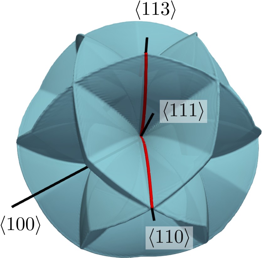
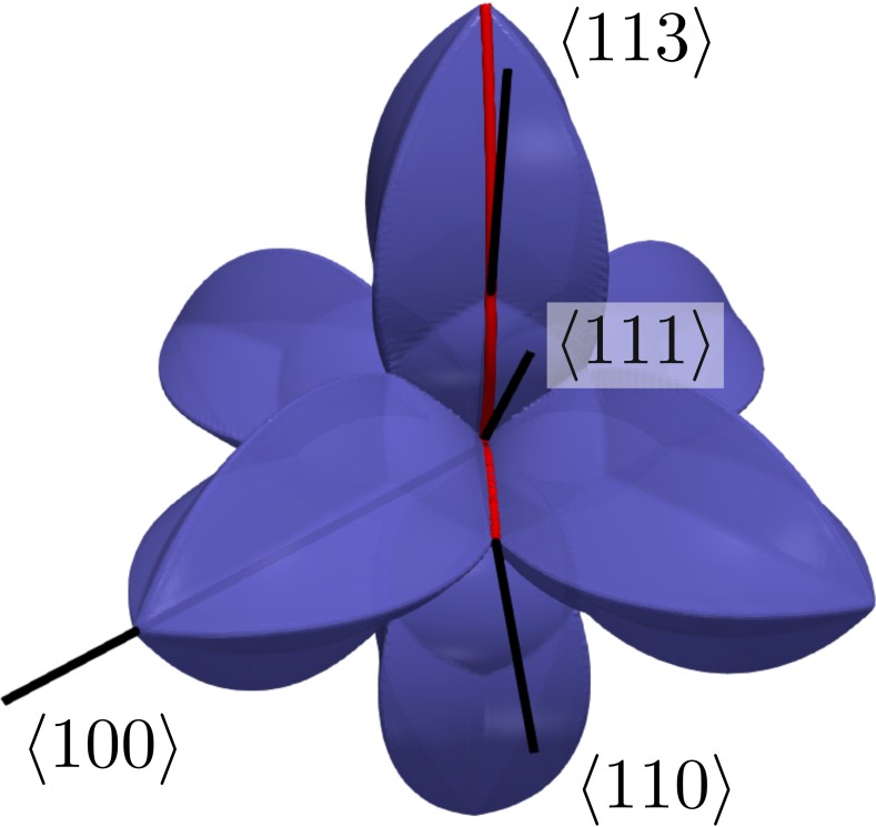
 for cubic crystals. (a) and (b) 3D illustration of , where the depicted surfaces are constructed from the function
  for all unit vectors
  . Additionally, slice paths are indicated (red lines). (c) and (d) Visualization of along the sliced paths. The distributions reflect octahedral symmetry (thus, they are typical for the case of wet etching of with ) and originate from Hubbard interpolation which is discussed in Section 5.1.1.
Reprinted with permission from Toifl et al., IEEE Access 8, 115406 [25] (2020). © 2020 Authors, licensed under the Creative Commons Attribution 4.0 License (http://creativecommons.org/licenses/by/4.0/).
Nevertheless, methods based on Wulff-Jaccodine are commonly employed to predict wet etching profiles. Due to the reaction-limited nature of anisotropic wet etching, surface reaction kinetics determines the etching rate and
well-defined orientation-dependent etch rate functions can be defined. Importantly, this framework is very similar to stationary kinetic growth models presented in Section 2.2.5. The first procedures to utilize the Wulff-Jaccodine method to simulate the etch profile evolution in 2D have resorted to polygonal
descriptions of the etch front [116], [117].
In recent years, the level-set method has been widely employed for anisotropic etching problems [25], [33], [118]–[122].
An important merit is that etch rate functions of the form can be directly incorporated into the level-set framework. In particular, the etching evolution is solely determined by a continuous , where every crystal orientation is assigned a etch rate  , which is exactly what is needed for the surface propagation equation (2.12). Furthermore, can be deduced from experiments and the wagon-wheel masking patterns and hemispherical specimen etching techniques are ideally suited to determine with high resolution with respect to crystal orientation.


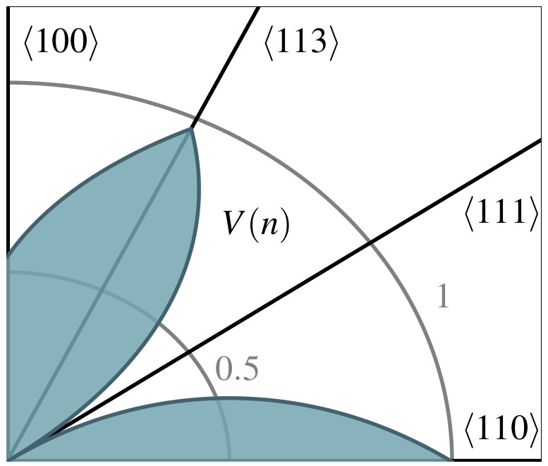
 ). (a) Prototypical evolution for as shown in Fig. 3.3a.
  is significantly larger than
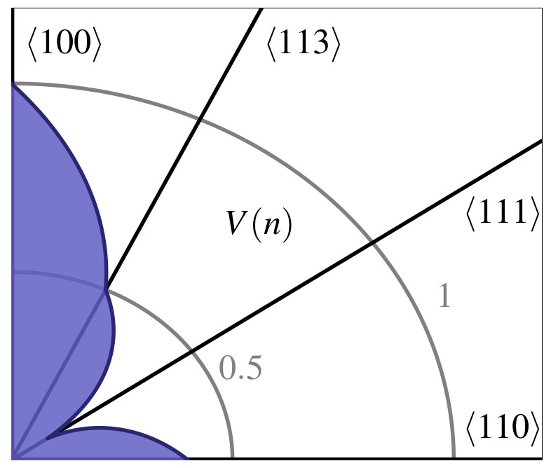
  , which causes planes to dominate already in the early phases. (b) Typical evolution for as shown in Fig. 3.3b. constitutes a local minimum and
  facets are (meta) stable before eventually define the etch profile. Even though the ultimate profiles look the same, the intermediate topographies differ.
Anisotropic wet etch profiles are typically characterized by a few defining facets, e.g., for . This is due to the fact that these characteristic facets are associated with minima and maxima of and thus define the limiting shape of the etch profile (consistent with Batterman’s rule). Fig. 3.3 shows two example distributions, which have a global
minimum at in common. This facet is eventually the dominating one, since most etching experiments naturally produce concave topographies (see Fig. 3.1).
Nevertheless, in experiments also high index facets can be (temporarily) observed. These facets represent local minima and are thus stable for a certain time before they disappear in favor of the global extrema facets. The impact of
the etch rate distribution is illustrated in Fig. 3.4, where the etch profile is shown for multiple etch times. The etching configuration is a standard etching
experiment where a masked substrate is locally exposed to the associated etchant. The resulting profile as visualized in Fig. 3.4a originates from the
distribution in Fig. 3.3c and is characterized by the fast emergence of the limiting shape (V-shape). In contrast, the etch profile evolution depicted
in Fig. 3.4b results from the distribution shown in Fig. 3.3d which is
characterized by a local maximum for facets. Hence, facets appear for a limited time. Similar observations can be made with a higher number of temporally appearing facets. The result is a topography that is potentially highly complex for certain stages of the etch process,
while the final topography converges to simpler geometries determined by a certain (mostly small) set of limiting rates. Modeling decisions are necessary here: If all details of the etch profile evolution (in particular during early
stages) are desired, a large number of facets and their corresponding etch rates need to be characterized. If the end result/later stages are sufficient, a significantly lower number of facets is viable. Even if elaborate characterization
data is available, interpolation techniques are necessary to generate the functional form of , see Chapter 5.
3.3 Summary
In this chapter, the fundamentals and modeling approaches of anisotropic wet etching were reviewed. Tab. 3.2 provides an overview of modeling techniques investigated in the literature.
Similar to the discussion of level-set based modeling of selective epitaxy in Section 2.2.5, level-set based simulations of anisotropic
wet etching were identified to be well-suited for semiconductor device engineering applications. The field of applicability is even wider compared to the epitaxy case, because a distribution can describe the broad field of reaction-limited wet etching processes.
Even though the level-set method is a powerful foundation for topography-based process simulation, the strong spatial dependence of , as illustrated in Fig. 3.3, presents numerical challenges. Since the local orientation depends on the local topography of the wafer, numerical inaccuracies in the description of the wafer surface have significant impact on etch or growth rates evaluated at every point of the surface. As a result, it is
important to ensure numerical stability and robustness. Hence, numerical schemes which enable reliable level-set simulations of anisotropic wet etching and SEG are presented in the following chapter.
| Physics/Chemistry | Surface Tracking | Application Targets | Dimension | Publications |
| Atomistic (KMC) | Discrete Interface | Morphology | 2D, 3D | [95], [107], [108], [112] |
| Atomistic (CCA) | Morphology, Topography | 3D | [109], [110] | |
| Continuum | Equilibrium Dynamics | Topography | 2D | [44], [116] |
| Phase-Field | Morphology | 3D Etching of Flat Initial Surface | [115] | |
| Level-Set | Topography | 3D | [25], [33], [118]–[122] |