

6 Process TCAD and Semiconductor Device Design
By integrating models for all important process steps in semiconductor fabrication (e.g., deposition, etching, and doping), a process simulator is capable of predicting a virtually fabricated semiconductor device model (in the form of a (volume-)discretized geometry) by employing a sequence of simulated fabrication steps: This device model captures the geometry and material properties of the semiconductor material stack which defines the device. The electrical or optical properties of the device are subsequently predicted by a device simulator which is a further central software tool in TCAD.
After focusing on the individual process steps in the previous chapter and to set the stage for the remainder of this work, a broader perspective on process TCAD and its well-known importance is highlighted. First, the general role of process TCAD in semiconductor device design is discussed. Second, the matured strategy of linking process and device simulations to provide further insights and optimization capabilities to facilitate the fabrication of efficient semiconductor devices is examined. This is illustrated with the example of post-implantation annealing of 4H-SiC-based power MOSFETs [181], where the optimal annealing process conditions to achieve the desired MOSFET characteristics are important.
In the final and main part of this chapter, the fabrication of  -based LEDs is discussed to motivate this particular area of application. Here, 3D patterning of the sapphire substrate is highly beneficial to optimize the optical efficiency of the LEDs. This is achieved with anisotropic
wet etching of sapphire, where particularly complex 3D topographies emerge. Hence, the developed numerical CA engine (Chapter 4) and continuum model for sapphire etching (Section 5.4), which
have both been proposed in this thesis, are employed and shown to be integral components for the necessary coupled process and device simulations: These coupled simulations provide the optimal wet etching process parameters to
fabricate -based LEDs with maximal optical efficiency.
-based LEDs is discussed to motivate this particular area of application. Here, 3D patterning of the sapphire substrate is highly beneficial to optimize the optical efficiency of the LEDs. This is achieved with anisotropic
wet etching of sapphire, where particularly complex 3D topographies emerge. Hence, the developed numerical CA engine (Chapter 4) and continuum model for sapphire etching (Section 5.4), which
have both been proposed in this thesis, are employed and shown to be integral components for the necessary coupled process and device simulations: These coupled simulations provide the optimal wet etching process parameters to
fabricate -based LEDs with maximal optical efficiency.
6.1 Linking Process and Device Simulation
As hinted before, in the general context of TCAD, process simulation is typically employed to generate a geometric device model that is provided to a device simulator. A device simulator predicts electrical and optical characteristics of semiconductor devices (e.g., voltage-current relations) by utilizing physical models for carrier transport, interface effects, and material properties. For many device structures the exact geometry of semiconducting and isolating layers impacts the device characteristics in intricate ways. Depending on the quality requirements, several options to achieve a viable device model can be employed. The simplest approach is to design the device model’s geometry with the help of 3D computer-aided design software (solid modeling approach). Some software tools provide the option for process emulation which uses sequential geometric options for etching/deposition and doped region creations. Hereby, it is possible to support deposition and removal of layers with a certain thickness or film conformality. This enables intuitive creation of device models and allows for rapid-prototyping, since the device model is built on the basis of lithography masks, critical dimensions, and more involved structures like spacers which naturally result from the mask layout. In contrast, the term process simulation in a rigorous sense is usually used if physical phenomena or chemical reactions are modeled on the feature scale, with the goal to predict etch profiles, film deposition geometry, or doping wells.
Semiconductor devices are fabricated with a large number of individual fabrication steps. As demonstrated in Chapter 5, emulation and simulation techniques can be employed alongside to generate a device model. Some processes are well-controlled and result in simple topographies (e.g., perfectly planar epitaxy), which can thus be addressed with emulation. Other processes involve physical/chemical processes leading to complex topographies or doping profiles. Process simulation is beneficial here, in particular, if the impact of process parameters on device characteristics is of interest [182].
Post-Implantation Annealing of 4H-SiC DMOSFETs
In order to illustrate the benefits of combined process and device simulations, the post-implantation annealing of 4H-SiC double-implanted MOSFETs (DMOSFETs) is considered [181]. High temperature annealing is required to electrically activate implanted dopants. Only if dopants are appropriately incorporated into the 4H-SiC crystal, they contribute free electrons and holes. This is achieved with a temperature step which induces a beneficial change of the atomic configuration of the implanted impurities. On a device level, optimized transistor channels are formed with n- and p-doped well implantation. Thus, electrical activation influences important parameters like on-state resistance and threshold voltage [40]. As a consequence, post-implantation annealing process parameters directly affect the performance of the final device.
Reprinted with permission from Toifl et al., IEEE Transactions on Electron Devices 66 (7) (2019), pp. 3060-3065 [181], © 2019 IEEE.
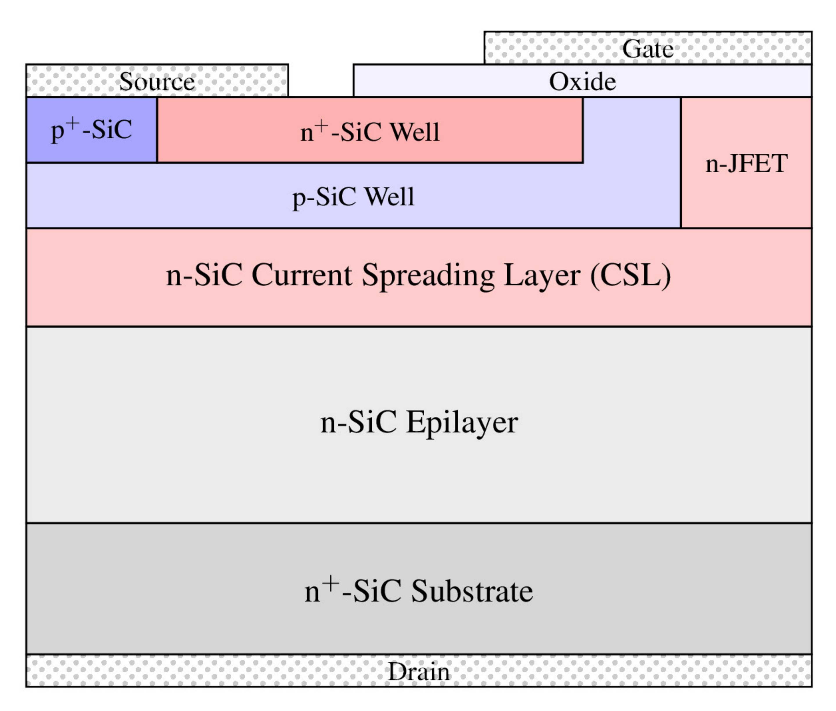
A 4H-SiC DMOSFET is a vertical power device structure shown in Fig. 6.1. In the following a low-voltage short channel
realization as presented by Saha et al. [183] is considered. After implantation of acceptor-type aluminum (p-SiC well) and donor-type
phosphorus (n-SiC well) a post-implantation annealing step at temperature  is performed for a specific annealing time
  . A transient annealing model has been proposed for aluminum- and phosphorous-doped 4H-SiC [184]. The time evolution of the electrically active dopant concentration
  depends on the activation reaction rate

 is the active dopant concentration in the steady state

which is determined by the total implanted concentration  and
and  ; the latter is a parameter related to the solid solubility of the respective impurity in 4H-SiC. The model parameters and follow an Arrhenius law

with an exponential prefactor  , activation energy
  , and Boltzmann constant
  . Model parameters have been calibrated to a large number of experiments presented in the literature: The experiments cover annealing steps of ion-implanted planted aluminum and phosphorous impurities in 4H-SiC,
which have been performed at various annealing temperatures, times, and total implanted concentrations [181], [184].
. Model parameters have been calibrated to a large number of experiments presented in the literature: The experiments cover annealing steps of ion-implanted planted aluminum and phosphorous impurities in 4H-SiC,
which have been performed at various annealing temperatures, times, and total implanted concentrations [181], [184].

Since the model parameters for aluminum and phosphorous differ, the ratio of active dopants differs for p- and n-doped regions for given annealing conditions. As a consequence, the difference of net doping of p- and n-wells is not
only determined by the implantation process via , but also by the post-implantation annealing process. The impact of the implantation and post-implantation annealing process on the device characteristics can be studied by coupling the process and device simulations.
Process simulation is performed with Silvaco Victory Process [140], where the following process steps are
considered to construct a model of the DMOSFET:
-
1. Planar epitaxial growth of a lightly n-doped 6 µm epitaxial layer
( ).
).
-
2. Planar epitaxial growth of a
 n-doped layer (
  ). This layer forms the current spreading layer (CSL) and the junction FET (JFET) region in the final device.
-
3. Deposition of the implantation mask (
 ).
).
-
4. Ion implantation of aluminum and phosphorous to form the p-well, highly doped n-well, and the highly p-doped region below the source contact. The implantation energies are chosen to produce a p-well with a depth of
 .
.
-
5. Annealing step, characterized by
and , using the activation model (6.1) and (6.2). The surface is capped with  .
.
-
6. Thermal oxidation to form the gate oxide with a thickness of 50 nm.
-
7. Metal deposition to form the contacts (source, gate, and drain).
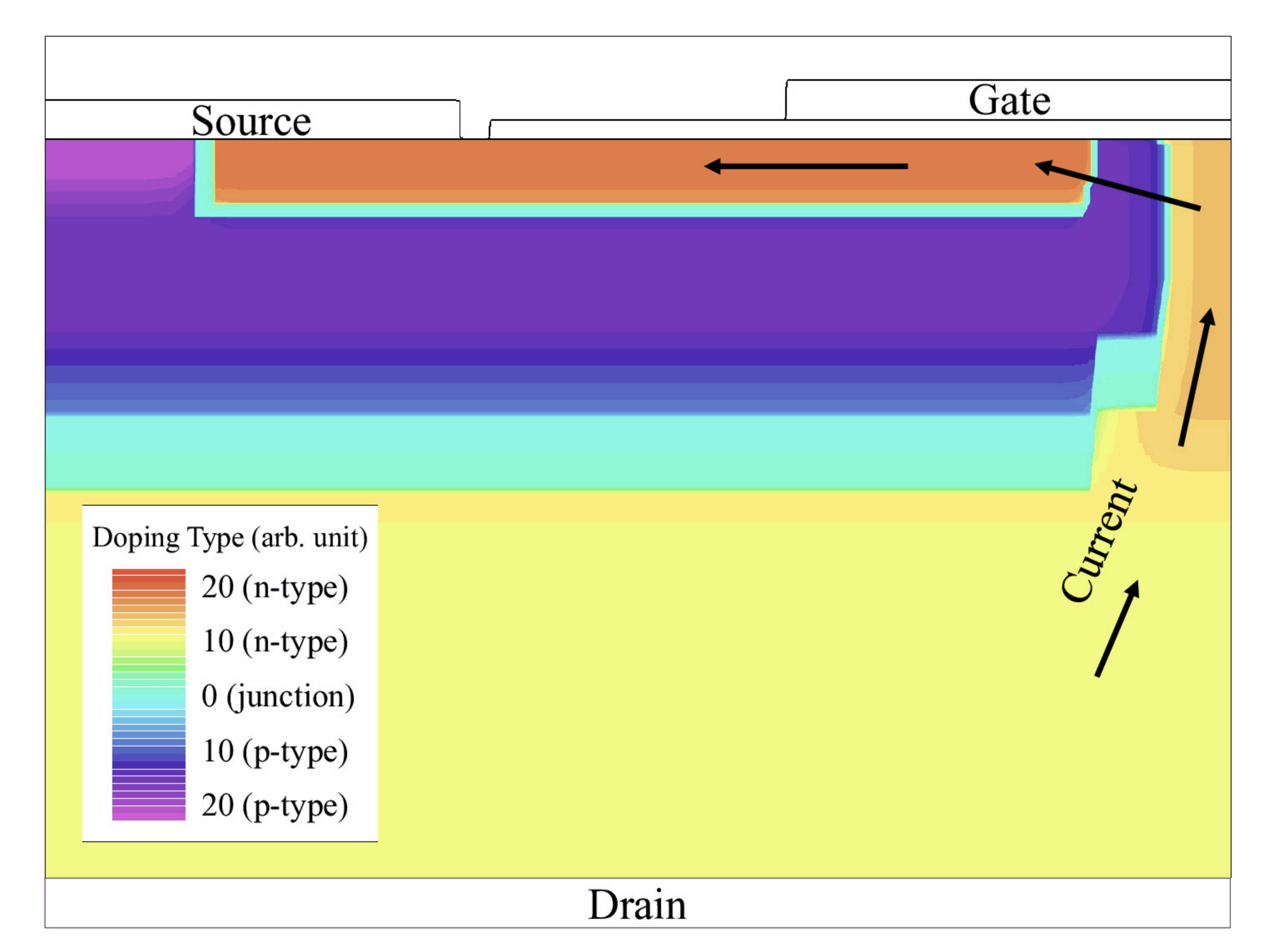
The result is a 2D model of the DMOSFET as shown in Fig. 6.1b. In particular, the active doping concentration in the p- and
n-doped wells is a function of annealing time and temperature. The structure is forwarded to the semiconductor device simulator Silvaco Victory Device [140], [181], which creates the ability of a coupled process and device workflow (shown in
Fig. 6.2). The device simulator is configured in drift-diffusion mode with Fermi-Dirac statistics. Two-level incomplete ionization [185], the Uhnevionak combined mobility model [186], and the
temperature-dependent bandgap model by Varshni [187] (calibrated according to experimental studies [188]) are employed. Shockley-Read-Hall [189] and Auger recombination [190] as well as impact ionization [191], [192] is used. Furthermore, the material interface between 4H-SiC and is characterized by interface state densities, which are typically two orders of magnitude higher than densities associated with a Si- interface [193].

Reprinted with permission from Toifl et al., IEEE Transactions on Electron Devices 66 (7) (2019), pp. 3060-3065 [181], © 2019 IEEE.
The device simulation setup is used within a coupled simulation workflow (Fig. 6.2). The DMOSFET model is fabricated with specific annealing temperature and time, which enables the investigation of the impact of post-implantation annealing process parameters on the threshold voltage of the final device. A phase plot of the threshold voltage as a function of annealing temperatures in the range from 1500 °C to 1750 °C and annealing times up to 8 min is shown in Fig. 6.3. The results confirm that the viability of DMOSFETs is significantly influenced by the annealing conditions. This is further reinforced by the gray-colored regions in Fig. 6.3, which correspond to the set of annealing variables resulting in purely resistive devices. These are lacking gate control capabilities and are thus not usable. For the functioning DMOSFETs, the threshold voltage is mainly determined by the active aluminum concentration in the channel. Thus, annealing time and temperature have a strong impact on the transfer characteristics. For instance, at a constant annealing temperature of 1600 °C, enhancing the annealing time from 3 min to 7 min causes a threshold voltage shift of approximately 3 V. A shift of the threshold voltage affects the switching beviour of the DMOSFET and thus needs to be carefully considered in the design of power switching circuits [40].
Closely coupled process and device simulations have been demonstrated to be highly beneficial for the optimization of post-implantation annealing parameters with respect of the final device properties of 4H-SiC DMOSFETs. In the next section the focus is shifted to a similar approach for the topography-focused optimization of LEDs.
6.2 Light Extraction Efficiency of GaN-Based LEDs
In this section -based LEDs on sapphire substrates are considered. The fundamental operating principles are introduced in order to discuss the impact of the topography of PSSs. These principles are applied to design combined process
and device simulations, which thereby provide the ability to optimize the parameters of the anisotropic wet etching process during the fabrication of PSSs.
A schematic illustration of a simplified double-heterojunction LED is presented in Fig. 6.4. The LED consists of back reflector
(silver), a sapphire substrate, confinement layers, an active region (stack of several alloys, e.g.,  and
and  ), a transparent current spreading layer (e.g., indium tin oxide (ITO)), and metal contacts. By applying an electrical bias across the pn-junction formed by p- and n-doped layers, carriers are injected into the active area, where they optically recombine and emit light. The active region is typically formed by multiple quantum wells to achieve emission of light with specific wavelengths.
Furthermore, the emitted light is undirected, i.e., the initial propagation direction is random [163].
), a transparent current spreading layer (e.g., indium tin oxide (ITO)), and metal contacts. By applying an electrical bias across the pn-junction formed by p- and n-doped layers, carriers are injected into the active area, where they optically recombine and emit light. The active region is typically formed by multiple quantum wells to achieve emission of light with specific wavelengths.
Furthermore, the emitted light is undirected, i.e., the initial propagation direction is random [163].

-based LED. By applying an electrical bias, carriers are injected into the active region where they radiatively recombine. Light is emitted in an undirected manner and traverses through the device. The refractive index of
the layers is larger than the indices of sapphire and the surrounding air. Hence, the LED acts as a waveguide, where a substantial fraction of light is not extracted due to total internal reflection (TIR). Additionally, contacts
are a major source of electromagnetical losses. The concept of extraction cones, which visualizes the set of incoming angles allowing for transmission at a material interface with  , can be generalized for a LED structure to characterize the fraction of light which is extracted from the device.
6.2.1 Ray Optics Approximation
The basic operating principle of LEDs can be explained within the ray optics approximation. The dimensions of a typical LED chip are significantly larger than the wavelength of the emitted light. Thus, it is possible to
approximate light propagation using ray optics, where light propagation is described with straight-line paths (in homogeneous media) and diffraction and interference phenomena are neglected [194]. The trajectory of light rays is determined by the refractive indices  of the media the rays traverse. When a light ray encounters a material interface (i.e., an abrupt spatial change of refractive index), a part of the electromagnetic wave is reflected and a part is refracted.
The propagation direction of the reflected ray is given by the law of reflection

where  denotes the angle between ray and interface normal. The incoming ray is indicated by the superscript
  and the reflected ray is specified with the superscript
  . The refracted component is described with Snell’s law [194]

Here,  denotes to the transmitted ray. The relative magnitude of the reflected and refracted components are given by the Fresnel equations [195], which provide the electromagnetic intensities of refracted and transmitted light. If a ray transitions from a medium with higher refractive index into a region
with lower refractive index (i.e., ) TIR can occur. This is the case if the incoming angle is larger than the critical angle
denotes to the transmitted ray. The relative magnitude of the reflected and refracted components are given by the Fresnel equations [195], which provide the electromagnetic intensities of refracted and transmitted light. If a ray transitions from a medium with higher refractive index into a region
with lower refractive index (i.e., ) TIR can occur. This is the case if the incoming angle is larger than the critical angle 

TIR limits the set of incoming rays which can traverse the interface. The associated  can be visualized with the concept of extraction cones (illustrated in Fig. 6.4): At an interface with
  , the set of incoming rays which are (at least partially) transmitted constitute the extraction cone.
During light propagation in matter, electromagnetic power is absorbed by the material. As a consequence, the intensity of light rays is attenuated. In other words, the material is lossy, which is modeled by introducing a
non-zero imaginary part  for the refractive index
  . In a lossy material the electromagnetic intensity
  exponentially decreases in space

where  refers to the propagation distance. The relation between the absorption coefficient
  and the is derived with the assumption of ideal plane waves with wavelength
  1. The metal contacts of an LED are usually the most pronounced source of losses.
Light propagation in LEDs can be well-described with these concepts. Semiconductors have refraction indices which are typically larger than 2, e.g., ![\( n_\mathrm {GaN}\approx \num [round-precision=1]{2.5} \)](PhD_Thesis-images/A04FDD45A3A8EFBEA669A68AE8D492B0.svg) . Since the surrounding air has a lower refraction index (
. Since the surrounding air has a lower refraction index (  ), layered semiconductor structures essentially act as waveguide. Only a certain fraction of rays can leave the LED, while the remaining rays are repeatedly (total internally) reflected until they are eventually entirely
attenuated. Thus, the geometry of the device intrinsically limits the amount of extracted light.
), layered semiconductor structures essentially act as waveguide. Only a certain fraction of rays can leave the LED, while the remaining rays are repeatedly (total internally) reflected until they are eventually entirely
attenuated. Thus, the geometry of the device intrinsically limits the amount of extracted light.
Even though the ray optics approximation is justified for large-scale LEDs, it is important to note that ray optics cannot be applied if the geometric features of the LED are smaller than the wavelength of emitted light in the active
region. If the geometric features of the LED are further reduced in size, it is more appropriate to treat these as surface roughness instead of topography features (typical blue-light LEDs emit in the spectral range from 0.4 µm to 0.55 µm [196]). If it is desired to consider surface roughness, specialized and typically significantly more complex models based on light scattering must be
employed [197].
1 Ideal plane waves are a reasonable approximation of collimated ray-like waves if the cross-section of the light beam is much larger than [195].
6.2.2 Light Extraction Efficiency
In general, the efficiency of LEDs refers to the capability of transforming electrical input power into radiant optical flux2. There are multiple contributions to the total efficiency [35], [163]

where  refers to the electrical efficiency (ohmic losses in contact, carrier injection efficiency). The internal quantum efficiency (IQE) quantifies the efficiency of photon generation inside the LED based on injected electrical
carriers. The so-called light extraction efficiency (LEE) describes the number of photons ultimately leaving the structure with respect to the number of internally generated photons. LEE is a function of the geometrical structure of
the LED and material properties (refractive indices) of the individual layers. The geometry-focused process modeling approach discussed in the previous chapters is well-suited to support the LED design. Hence, LEE is discussed in
detail in the following.
refers to the electrical efficiency (ohmic losses in contact, carrier injection efficiency). The internal quantum efficiency (IQE) quantifies the efficiency of photon generation inside the LED based on injected electrical
carriers. The so-called light extraction efficiency (LEE) describes the number of photons ultimately leaving the structure with respect to the number of internally generated photons. LEE is a function of the geometrical structure of
the LED and material properties (refractive indices) of the individual layers. The geometry-focused process modeling approach discussed in the previous chapters is well-suited to support the LED design. Hence, LEE is discussed in
detail in the following.
A geometrical picture of LEE is the effective light extraction cone, as depicted in Fig. 6.4, which is characteristic for the entire
LED. In order to achieve highly efficient LEDs, the light extraction cone needs to be as wide as possible, i.e., to allow for maximal light extraction at the chip surfaces. A plethora of techniques to improve LEE has been proposed
and implemented. The most well-known technique is high-index encapsulation, where the LED chip is encapsulated in a medium that has a refractive index between air and semiconductor. For instance, dome-shaped epoxy resin
encapsulation (epoxy dome) with  is employed to enlarge the extraction cone. By reducing the refractive index contrast the critical angle is increased. Furthermore, the global geometry of the chip can be optimized (chip shaping). The ideal chip shape is a point-like emitting region [35], which is not feasible in practice. Hence, many shapes have been studied in the past to optimize efficiency: Triangular, slanted geometries, truncated inverted
pyramids [198], and more advance concepts like sidewall-deflector-integrated LEDs [199].
is employed to enlarge the extraction cone. By reducing the refractive index contrast the critical angle is increased. Furthermore, the global geometry of the chip can be optimized (chip shaping). The ideal chip shape is a point-like emitting region [35], which is not feasible in practice. Hence, many shapes have been studied in the past to optimize efficiency: Triangular, slanted geometries, truncated inverted
pyramids [198], and more advance concepts like sidewall-deflector-integrated LEDs [199].
It is also possible to make use of the wave nature of light and employ optical mode quantization in microcavities and photonic crystals [200].
Textured or patterned interfaces are particularly interesting for -based LEDs [163]. Complex substrate topographies, as shown in Section 5.4 with PSS, introduce strong ray trajectory variations to the LED. The irregularity of interfaces provides the possibility of enlarging the effective extraction cone by reducing the
amount of rays which are total internally reflected at the chip edges. In the ideal case, the trajectories of light rays can be altered to pass the TIR criterion (6.6) after interacting with non-planar -PSS interfaces.
2 A related quantity which is also often used is the luminous efficacy (given in units of lm/W), where the power efficiency is weighted by the spectral sensitivity of the human eye.
Light Extraction Efficiency Ray-Tracing
LEE optimization of LEDs can be supported with computational methods. The previously discussed ray optics approximation is directly employed in ray-tracing simulations [163], [201], [202], which are referred to as LEE ray-tracing (LRT) methods in the following. The main idea of LRT is to follow the propagation of light rays as they traverse through the LED. In order to model undirected emission, rays are set up at random positions in the active region with randomized initial propagation direction. If a ray hits a material interface, the law of reflection (6.4) and Snell’s law (6.5) is applied, which results (in the general case) in two rays being traced: A reflected and a refracted ray. Furthermore, the generated light in a LED is not a perfectly collimated light beam, i.e., the light ray spreads spatially during propagation (beam divergence). This leads to situations where the material interface that is hit by a ray is not sufficiently characterized by a single interface normal. In LRT methods, this is accommodated for by splitting the incoming ray into two rays, which interact with the interface via two interface normals [203]. Hence, the number of light rays that are traced are gradually increased on non-planar interfaces, even if only TIR occurs. Additionally, attenuation during propagation is modeled with (6.7), which results in a reduction of the optical power assigned to the ray.
The ultimate goal of LRT is to compute the amount of optical power which is not dissipated within the device and thus contributes to the far (radiant) field. LRT enables the investigation of LED designs with high flexibility regarding the geometry of the device structure: In the literature, several chip shapes, contact geometries, interface textures, and the impact of surface roughness have been studied [35], [163]. As far as interface texturing is concerned, typically idealized geometries are considered, e.g., regular arrays of cones. In the following, the effect of complex PSS topographies fabricated with anisotropically wet etching are investigated.

-based LED with PSS (top, not to scale) and typical dimensions as presented in the literature [163],
[174]. A dome-shaped encapsulation with epoxy resin is implied. In order to investigate the impact of PSS topography, a periodic unit cell which does not include
contact pads is considered (bottom). The unit cell has periodic boundaries at the sidewalls and a reflective boundary at the bottom. In LRT simulations, an isotropic distribution of rays is initiated in the active region (labeled
as ) and the paths of the rays through the structure are traced. Snell’s law (6.5) is applied at material interfaces
and the number of rays leaving the structure is determined by the simulation.  ,
,  , and
, and  illustrate ray paths which result in extracted light.
6.2.3 Coupled Process and Device Simulations
In order to demonstrate the impact of wet etching process parameters on the LEE of -based LEDs, a representative LED device structure is considered (depicted in Fig. 6.5). The active region is labeled , as it is typically composed of multiple and quantum wells. The backside mirror enforces mainly top-facet emission and encapsulation with epoxy resin (i.e., epoxy dome) enlarges the extraction cone [163]. The geometric features of the PSS are periodic, where the periodic unit cell has dimensions which are significantly smaller than the entire LED.
In the following, the discussion focuses on the the impact of the PSS topography on LEE. Hence, the exact device dimensions (apart from the PSS topography) and contact pad arrangement are assumed to be already optimized.
The impact of the PSS topography can be isolated by considering only a periodic unit cell (lower illustration in Fig. 6.5). Ray
propagation in the unit cell is modeled with periodic lateral boundaries, i.e., the edges of the LED are not considered, and a reflecting bottom boundary (mirror). Thus, rays can only leave the structure via the top. Furthermore,
three prototypical traces of light rays ( , , and ) in the periodic unit cell are depicted in Fig. 6.5 (lower image): is initially propagating towards the bottom of the device, but is reflected twice at the -PSS interface by means of TIR, which ultimately results in light extraction. demonstrates direct emission, which is independent of the substrate pattern. Furthermore, illustrates interaction with the periodic domain boundaries.
Process Simulation Setup
Since the exact topography of the -PSS interface depends on the etching process parameters (etchant mixture, etch temperature, and time), coupling the anisotropic wet etching model of Section 5.4 with LRT allows for optimization of the process parameters etchant mixture, etch time, and temperature. Fig. 6.6 illustrates the simulation flow to implement combined etching and LRT simulations. First, anisotropic wet etching is simulated with the proposed CA
engine (implemented in Silvaco Victory Process). The sapphire wet etching model M0-1 Tab. 5.5 is employed on the initial pre-patterned PSS structure, as
shown in Fig. 6.6 (I). The simulation domain is a 3D periodic unit cell of the PSS with periodic boundaries in the wafer plane and
a high resolution of  , which is required to resolve the intricate topography features.
After the etching simulation is performed with etch time and temperature  (Fig. 6.6 (II)) the stack of , , ITO is produced with idealized geometry operations (planar material regions with thickness given in Tab. 6.1),
forming a high-resolution periodic unit cell of the LED (Fig. 6.6 (III)). For the subsequent device simulation a Delaunay mesh [204] is required. Hence, the level-set representation of the cell is transferred to an explicit mesh using the marching cubes
algorithm [126]. However, the marching cubes generated mesh is not a Delaunay mesh, which is why the meshing tool Silvaco Victory Mesh [140] is employed to convert the mesh to a Delaunay tetrahedral mesh. Additionally, the structure of the resulting Delaunay mesh is optimized. The -PSS interface is resolved with high accuracy employing a linear grading in the characteristic size (i.e., diameter) of the mesh simplices. At the interface the characteristic size is 0.14 µm and at
1.68 µm distance from the interface, the size is 0.56 µm (Fig. 6.6 (IV)).
(Fig. 6.6 (II)) the stack of , , ITO is produced with idealized geometry operations (planar material regions with thickness given in Tab. 6.1),
forming a high-resolution periodic unit cell of the LED (Fig. 6.6 (III)). For the subsequent device simulation a Delaunay mesh [204] is required. Hence, the level-set representation of the cell is transferred to an explicit mesh using the marching cubes
algorithm [126]. However, the marching cubes generated mesh is not a Delaunay mesh, which is why the meshing tool Silvaco Victory Mesh [140] is employed to convert the mesh to a Delaunay tetrahedral mesh. Additionally, the structure of the resulting Delaunay mesh is optimized. The -PSS interface is resolved with high accuracy employing a linear grading in the characteristic size (i.e., diameter) of the mesh simplices. At the interface the characteristic size is 0.14 µm and at
1.68 µm distance from the interface, the size is 0.56 µm (Fig. 6.6 (IV)).

-based LEDs. The periodic unit cell is considered, as depicted in Fig. 6.5. The simulation flow involves a process simulator,
Delaunay meshing software, and a device simulator. (I) The conical PSS is generated with process emulation. (II) The continuum model for anisotropic wet etching of sapphire is employed to simulate the PSS topography
for a specific etchant, etch time, and temperature. (III) A series of planar epitaxy steps is used to form layers, active region, and ITO. (IV) The resulting high-resolution mesh is re-meshed to construct a Delaunay mesh with optimized -sapphire interface. (V) LRT is employed to calculate the LEE of the LED. As a result, the impact of wet etching parameters on LEE of the final device is quantified.
LRT Simulation Setup
LRT is performed with Silvaco Victory Device in LED mode (electrical carrier transport is not considered). The simulation setup is designed to focus on the impact of -PSS interface geometry on LEE. The goal is to capture the relative increase or decrease in LEE as a function of wet etching parameters. A periodic setup of the computational domain is employed with periodic boundaries
at the lateral edges of the unit cell. The ambient refractive index is set to  (epoxy). Therewith, it is assumed that every ray leaving the device structure and thus reaching the ambient region contributes to the extracted field. Equivalently, the shape of the epoxy dome is considered to be ideal,
i.e., there is no back reflection due to TIR at the epoxy-air interface. Furthermore, the backside mirror is set up as an ideal reflective boundary without causing losses.
(epoxy). Therewith, it is assumed that every ray leaving the device structure and thus reaching the ambient region contributes to the extracted field. Equivalently, the shape of the epoxy dome is considered to be ideal,
i.e., there is no back reflection due to TIR at the epoxy-air interface. Furthermore, the backside mirror is set up as an ideal reflective boundary without causing losses.
Light rays are generated at 16 homogeneously distributed points  in the active region. For each point , 360 initial ray directions are used to sample the emission sphere, as indicated in Fig. 6.5. The total generated (internal)
optical power is normalized to
in the active region. For each point , 360 initial ray directions are used to sample the emission sphere, as indicated in Fig. 6.5. The total generated (internal)
optical power is normalized to  . The tracing of a ray is terminated if more than two reflections occur. This imposed limit of two reflection is motivated by a trade-off between accuracy and computation time. On the one hand, a terminated ray does not
contribute to the extracted radiant optical flux, even though it might be actually extracted after a larger number of reflections. On the other hand, the computation time exponentially increases with increasing number of reflections
before termination. This is caused by the ray splitting mechanisms discussed in Section 6.2.2. The particular choice of a limit of two
reflection enables the consideration of the typical ray path in Fig. 6.5 (lower image), which is characterized by a double reflection at the -PSS interface and contributes significantly to the LEE .
. The tracing of a ray is terminated if more than two reflections occur. This imposed limit of two reflection is motivated by a trade-off between accuracy and computation time. On the one hand, a terminated ray does not
contribute to the extracted radiant optical flux, even though it might be actually extracted after a larger number of reflections. On the other hand, the computation time exponentially increases with increasing number of reflections
before termination. This is caused by the ray splitting mechanisms discussed in Section 6.2.2. The particular choice of a limit of two
reflection enables the consideration of the typical ray path in Fig. 6.5 (lower image), which is characterized by a double reflection at the -PSS interface and contributes significantly to the LEE .
The refractive indices of the LED layers, as reported in Tab. 6.1, reflect an emission wavelength  . Importantly, only real-valued refractive indices are employed. Thus, attenuation is entirely neglected, which is motivated by small dimensions of the unit cell. Rays that can leave the device typically travel a rather short
distance and the impact of attenuation is small. Moreover, due to the ray termination condition of two reflections, rays which are reflected multiple times back and forth (e.g., -PSS and mirror) before they leave the device are entirely neglected in any case. Even though neglecting absorption is a crude approximation, in particular for the large sapphire substrate, the calculated results are still
valuable to quantify the isolated impact of -PSS interface geometry on LEE in a relative sense. An important implication for the simulation domain is that a thin pseudo-substrate can be used, which consists of the PSS topography and a cuboid with small
extension in z-direction (Fig. 6.6 (IV)). Since absorption in the sapphire region is neglected and an ideal backside mirror is assumed, the
substrate thickness of typically
. Importantly, only real-valued refractive indices are employed. Thus, attenuation is entirely neglected, which is motivated by small dimensions of the unit cell. Rays that can leave the device typically travel a rather short
distance and the impact of attenuation is small. Moreover, due to the ray termination condition of two reflections, rays which are reflected multiple times back and forth (e.g., -PSS and mirror) before they leave the device are entirely neglected in any case. Even though neglecting absorption is a crude approximation, in particular for the large sapphire substrate, the calculated results are still
valuable to quantify the isolated impact of -PSS interface geometry on LEE in a relative sense. An important implication for the simulation domain is that a thin pseudo-substrate can be used, which consists of the PSS topography and a cuboid with small
extension in z-direction (Fig. 6.6 (IV)). Since absorption in the sapphire region is neglected and an ideal backside mirror is assumed, the
substrate thickness of typically  can be reduced to a minimal thickness, i.e.,
  3.
3.
 Since attenuation in the sapphire substrate is neglected, it is possible to significantly reduce the thickness of the sapphire substrate and still quantify the relative impact of the -sapphire interface on LEE.
| ITO | p-GaN | InGaN | n-GaN | GaN | PSS | Epoxy Dome | |
| Thickness [µm] | 0.25 | 0.2 | 0.01 | 2 | 5 | 1 |
|
| Refractive Index | 2.1 | 2.5 | 2.5 | 2.5 | 2.5 | 1.7 | 1.5 |

 . The LEE of the original conical PSS (0 min) is the reference for the provided relative LEE values. The LEE is maximal for an etch time of 18 min, which corresponds to an increase of 15% compared with
the conical PSS. Longer etch times result in a drop of LEE, which is mainly due to the increased fraction of planar topography as the PSS features are gradually etched away. The optimal PSS topography achieves a 77% increase in
LEE compared with a planar sapphire substrate, which highlights the significant impact of interface patterning on the LED performance.
. The LEE of the original conical PSS (0 min) is the reference for the provided relative LEE values. The LEE is maximal for an etch time of 18 min, which corresponds to an increase of 15% compared with
the conical PSS. Longer etch times result in a drop of LEE, which is mainly due to the increased fraction of planar topography as the PSS features are gradually etched away. The optimal PSS topography achieves a 77% increase in
LEE compared with a planar sapphire substrate, which highlights the significant impact of interface patterning on the LED performance.
3 Numerical experiments have been performed to calculate the LEE for different substrate thicknesses. The results confirm constant LEE if the number of completely traced rays is also kept constant.
Coupled Process and LRT Simulations
Coupled process and LRT simulations have been performed for the wet etchant M0-1 (  ) at 493 K. The relative LEE (normalized to the initial cone structure) is plotted for different etch times in Fig. 6.7. A gradual increase of relative LEE is shown until a maximum at 18 min is reached. Compared with the initial cone structure,
LEE is increased by approximately 15%. The corresponding -PSS interface topography is also depicted in Fig. 6.7. As etch time is increased to more than 18 min, the LEE
sharply drops, which can be explained by the increasing fraction of planar geometry. Planar regions have a detrimental effect, because they are parallel to the top facet of the device. Hence, due to TIR at planar regions of the -PSS interface the extraction cone of LED is effectively reduced. Accordingly, minimal LEE is observed for a completely flat -PSS interface (40 min). When comparing the optimized LEE with the LEE obtained for a planar interface, a notable 77% increase is observed. Thus, the significant impact of the -sapphire interface patterning on LEE is demonstrated, and the merits of PSS in general are corroborated. Nevertheless, the LEE is not solely explained by the fraction of planar regions, since the optimal topography (
) at 493 K. The relative LEE (normalized to the initial cone structure) is plotted for different etch times in Fig. 6.7. A gradual increase of relative LEE is shown until a maximum at 18 min is reached. Compared with the initial cone structure,
LEE is increased by approximately 15%. The corresponding -PSS interface topography is also depicted in Fig. 6.7. As etch time is increased to more than 18 min, the LEE
sharply drops, which can be explained by the increasing fraction of planar geometry. Planar regions have a detrimental effect, because they are parallel to the top facet of the device. Hence, due to TIR at planar regions of the -PSS interface the extraction cone of LED is effectively reduced. Accordingly, minimal LEE is observed for a completely flat -PSS interface (40 min). When comparing the optimized LEE with the LEE obtained for a planar interface, a notable 77% increase is observed. Thus, the significant impact of the -sapphire interface patterning on LEE is demonstrated, and the merits of PSS in general are corroborated. Nevertheless, the LEE is not solely explained by the fraction of planar regions, since the optimal topography (  ) is characterized by a larger flat area than the initial cone structure. The increase in LEE originates from the intricate redirection of light induced by the complex 3D PSS topography.
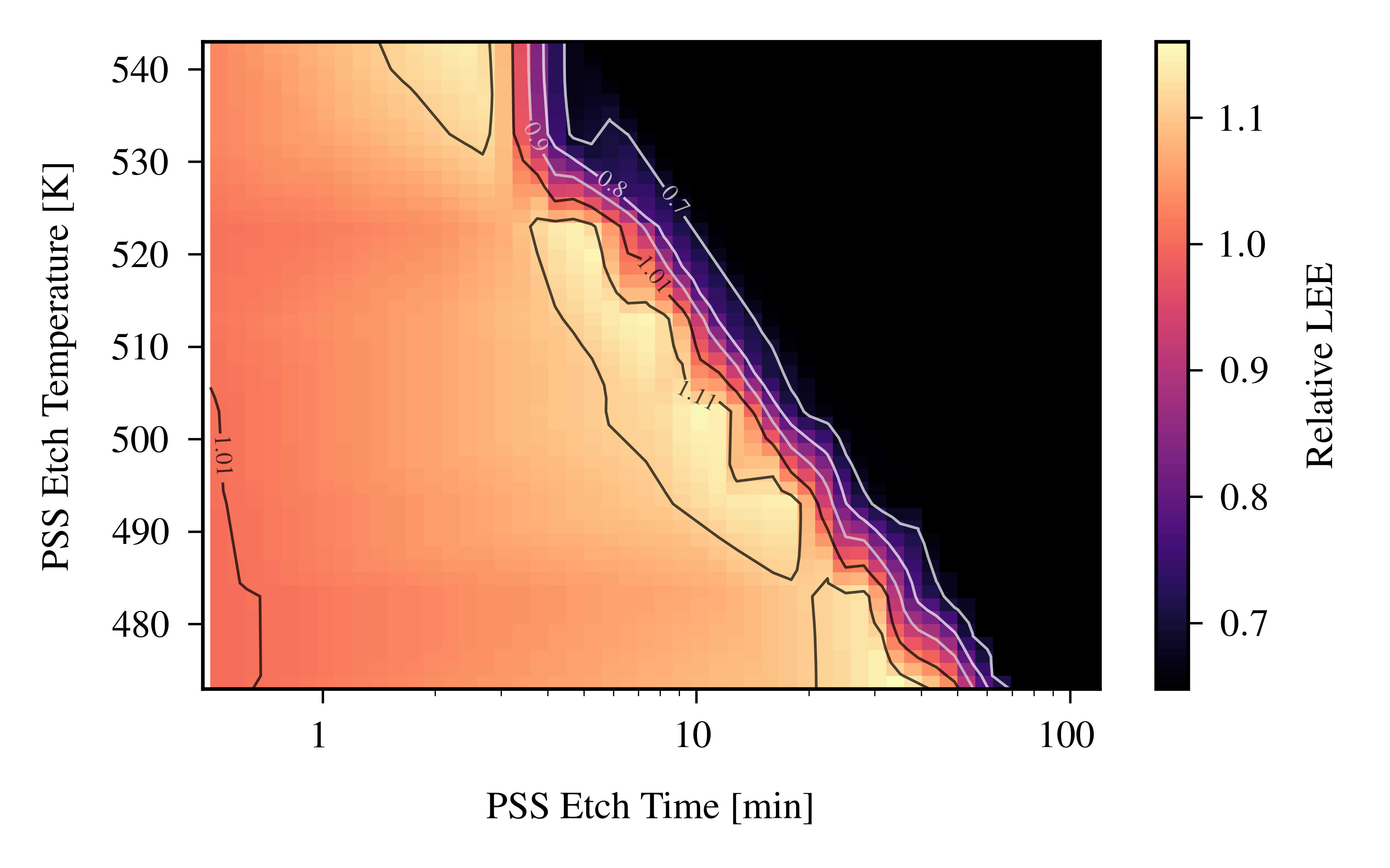
Aside from etch time, etch temperature also affects the topography of the PSS. Fig. 6.8 shows the relative LEE for several LEDs processed with etchant M0-1 in a semi-logarithmic phase plot. The etch time is displayed on a logarithmic scale and the etch temperature is given on a linear scale. The phase plot supports the identification of suitable etch parameters. On the one hand, elevated temperatures allow for smaller etch times, which is typically desired. On the other hand, the region of optimal LEE is broader on the time axis for lower temperature. Thus, etch stop mechanisms are not required to be as precise as in the elevated temperature case.
In summary, coupled process and LRT simulations enable advanced capabilities for the optimization of -based LEDs. The impact of complex topographies produced with anisotropic wet etching of sapphire is not entirely captured with simple models (e.g., fraction of planar regions on the -PSS interface). LEE calculation techniques benefit from the sapphire geometries provided by topography-focused process simulations, which also contribute a link to actual process parameters required to achieve certain
geometries.
6.3 Summary
In this chapter, closely coupled process and device simulations were presented. These provide the ability of a feedback loop of process and device TCAD models and techniques, enabling the optimization of process parameters by
computationally determining their impact on device performance. The post-implantation annealing of 4H-SiC DMOSFETs served as a general example for the benefits of this approach. Finally and most importantly, the numerical
techniques for 3D topography evolution proposed in Chapter 4 and the continuum model for anisotropic wet
etching of sapphire presented in Chapter 5 were employed to perform such coupled simulations in the context of -based LEDs. The impact of sapphire patterns on the optical efficiency of the final LED was quantified, which led to the identification of optimal etch process parameters (i.e., etch time and temperature).