

1 Introduction
The extraordinary complexity of modern day’s semiconductor devices has been greatly facilitated by simulation software. Motivated by the capability of reducing development time and costs, various tools have been developed to support different stages of the fabrication of electrical circuits and their components (e.g., transistors). When designing a semiconductor device, several challenges need to be addressed. The central question is the optimal geometrical structure and choice of materials to achieve a desired functionality, e.g., switching characteristics of a transistor. The set of possible device designs is limited by constraints imposed by the fabrication process: A feasible sequence of process steps, practical material systems, and appropriate equipment need to be feasible and reliable. Moreover, the development of novel semiconductor devices requires constant innovations in fabrication techniques and materials. When individual components are connected to each other, entire semiconductor systems, such as integrated circuits (IC), are formed. Here, interconnections and packaging have to be optimized to fabricate efficient and reliable systems.
All these facets of semiconductor fabrication are facilitated by computer simulation techniques, motivating the following classification of modeling approaches: Equipment-related, feature scale, and IC scale modeling (visualized in
Fig. 1.1). The term feature scale refers here to the level of individual components with its geometric features on the length scale of  or
or  . The feature scale simulation of semiconductor device fabrication as well as device and circuit operation is commonly referred to as technology computer-aided design (TCAD) [1]–[3].
In general, a semiconductor device is composed of a stack of several thin material layers built on a substrate (wafer). In device TCAD the electrical, optical, or mechanical operational characteristics of semiconductor devices are calculated given the geometry and material properties. Electrical simulations are concerned with the electrical operation of a device, including observable voltage and current levels on the external contacts. These are based on models which use different levels of electronic transport theory and electrostatics [4]. Light emission and absorption is essential in optoelectronic devices and is calculated with methods from (quantum) optics [5]. The mechanical properties of semiconductor materials are of interest for many actuators, sensors, and advanced transistors (strain engineering) and are modeled with continuum mechanics [6]. Furthermore, a profound understanding of phenomena like the thermoelectric [7] or the piezoelectric effect [8] is essential in the field of MEMS [9]. By utilizing these modeling techniques, device TCAD ultimately aims at predicting device behavior as seen from an abstracted external perspective, e.g., by predicting current-voltage characteristics under given operational conditions.

The characteristics of many semiconductor devices depend on the exact two-dimensional (2D) or three-dimensional (3D) geometry of all material layers. The range of technologically feasible geometries is affected by the details of the fabrication process. A typical semiconductor chip is manufactured by hundreds of individual process steps. In essence, these are based on processes which add material to the wafer (deposition), remove material from the wafer (etching), or change material properties (e.g., doping, annealing). The desired geometry is achieved using photolithography, where semi-transparent masks are utilized to transfer photoresist patterns to the wafer. Photoresist patterns act as masking regions which allow for spatial control of deposition, etching, and doping processes. By performing these processes in succession, a plethora of semiconductor device structures can be realized.
Motivational Fabrication Sequence
In order to illustrate the modeling of semiconductor fabrication processes, a simplified (but realistic) exemplary fabrication process is shown in Fig. 1.2. The process steps are designed to specifically pattern the surface of a sapphire wafer to achieve a 3D geometry which is beneficial for LEDs. Starting with a sapphire wafer (substrate), photoresist and hardmask (e.g., silicon nitride) layers are deposited. These layers protect certain regions of the substrate from the subsequent reactive ion etching (RIE) step, which results in a patterned sapphire surface. The sapphire wafer is subsequently processed by employing an etching step using wet chemistry, giving rise to the desired 3D surface topography.

The fabrication flow of Fig. 1.2 illustrates that different processes are required. Each of these processes is based on different underlying physical and chemical phenomena. While anisotropic wet etching is a wet chemical process, where the entire wafer is submerged in an etchant [11], RIE takes place in a low-pressure reaction chamber and utilizes plasma phenomena [12]. It can thus be clearly seen that semiconductor process modeling is a broad interdisciplinary field.
In general, there are two main perspectives on process modeling: An equipment-centered and a feature scale perspective. In the former, the entire reaction chamber and the equipment geometry is considered and the impact of equipment-level parameters (e.g., precursor gas flow) on deposition or etch rates is studied. Hereby, techniques from fluid dynamics and heat transfer modeling are used to describe pressure, temperature distribution, and (multi-step) chemical reactions in a reactor [13]–[15]. These approaches support the equipment design and, for instance, enable the prediction of the variation of deposition and etch rates across the wafer. Due to the large difference in length scale, micro features of semiconducting and isolating substrates and films are typically not described with equipment-focused modeling approaches.
In contrast, the second process modeling perspective (feature scale process modeling) is concerned with micro features which are small in extension compared to the reaction chamber [2]. The local surface topography and material properties are at the center of attention in order to characterize the time evolution of the wafer surface. In particular, the impact of process steps on essential geometry features and material properties are of importance. For instance, a slight misalignment of the photoresist pattern in the RIE step of Fig. 1.2 can cause a deviation of the resulting etch profile. Hence, variability is introduced, which is accumulated over multiple successive steps, and thus needs to be considered my means of processing tolerances or ultimately in the device design. Consequently, feature scale process modeling provides highly valuable information for device TCAD. A computer simulation based on these modeling approaches is referred to as semiconductor process simulation in this work and the field is generally known as process TCAD [1], [2].
Process TCAD
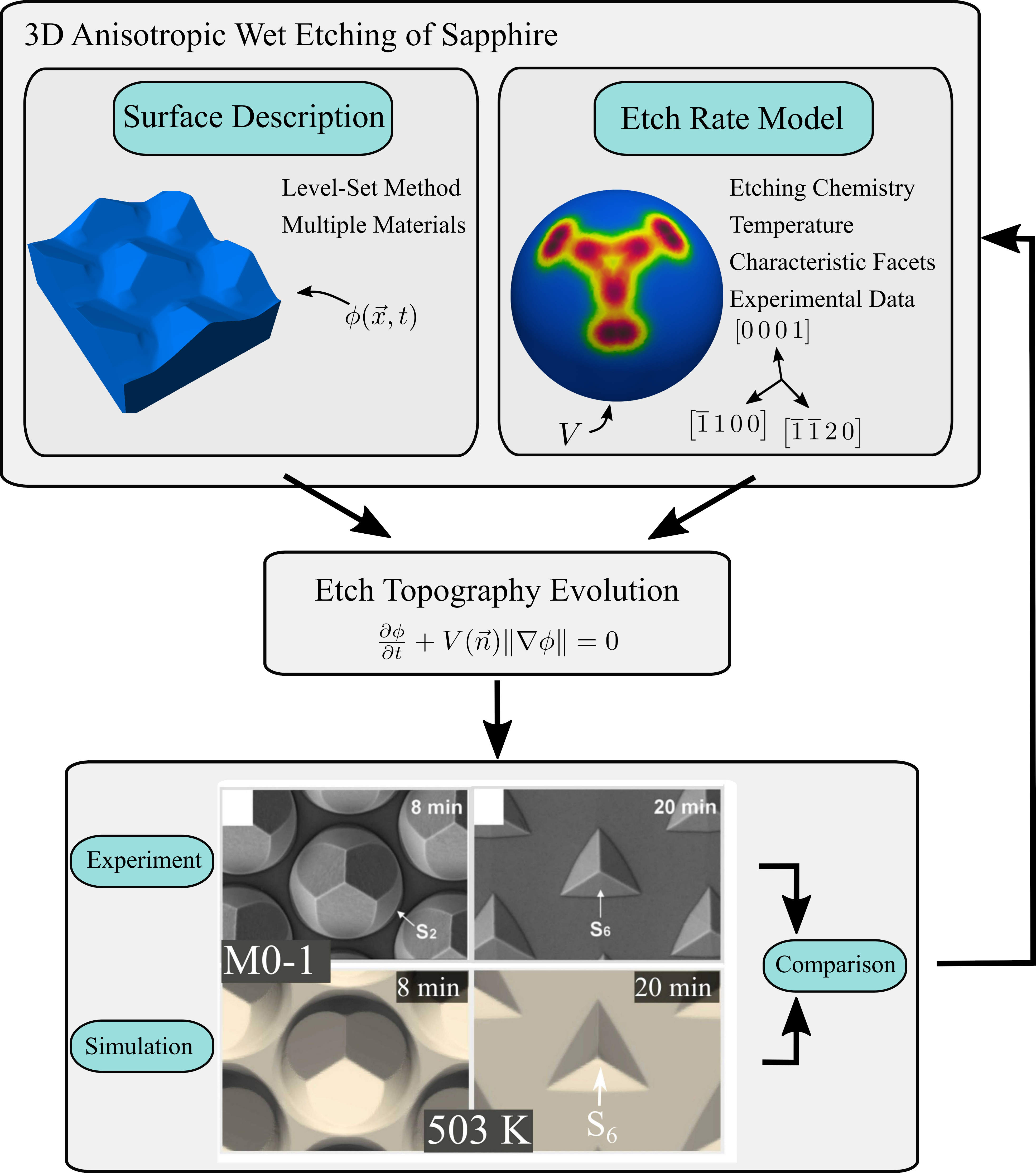
In order to outline the main challenges of process TCAD, the final wet etching step of the sapphire patterning process in Fig. 1.2 is considered. The etching removes material from the sapphire wafer and thus affects the wafer geometry. The removal rate is determined by the chemical reactions taking place on the wafer surface. An etch rate model describes the relation between the strongly orientation-dependent removal rate and process conditions. The process conditions are characterized by specific parameters which are in this case etch chemistry composition (i.e., etchant mixture) and temperature. Hence, three main components are important to develop a process model, as illustrated in Fig. 1.3:
-
• A method to describe the (potentially complex) 3D wafer surface geometry.
-
• A model describing how the wafer surface is changing during the process step.
-
• A method to move the surface according to the model (i.e., time evolution).
An important example for an elegant and convenient approach to describe complex 3D surfaces is the level-set method [16]. The level-set method is, aside from process TCAD, also widely employed in various computer simulations, including hydrodynamics [17], electroporation [18], and high-frequency wave propagation [19]. The surface geometry is (implicitly) described with a multi-dimensional function, the level-set function  . The elegance of this approaches comes from the ability to easily handle topological changes (such as coalescence of formerly separated islands) and from the uniform treatment of 2D and 3D geometries. These properties
are highly beneficial for the simulation of semiconductor fabrication processes. The level-set method also provides the ability to move the wafer surface via the level-set equation. In the example of Fig. 1.3, the wafer surface (described with ) is propagated according to the etch rate model yielding a surface velocity (denoted as
. The elegance of this approaches comes from the ability to easily handle topological changes (such as coalescence of formerly separated islands) and from the uniform treatment of 2D and 3D geometries. These properties
are highly beneficial for the simulation of semiconductor fabrication processes. The level-set method also provides the ability to move the wafer surface via the level-set equation. In the example of Fig. 1.3, the wafer surface (described with ) is propagated according to the etch rate model yielding a surface velocity (denoted as  ), which results in the etch profile after a certain etch time.
Since process TCAD directly supports device design, comparisons with experimental results are highly important. This motivates the empirical approach, where data from experiments, e.g., etch rates for specific crystal orientations, is incorporated into the modeling process. Usually, models with a minimal number of parameters are desired. Nevertheless, the most important topographical features need to be sufficiently resolved.
Selective Epitaxy and Anisotropic Wet Etching
Particularly complex typographical features are observed with inherently anisotropic processes which include selective (hetero-)epitaxial growth and anisotropic wet etching. The term inherently refers to direction-dependent deposition and etching processes which are caused by the crystalline structure that the majority of semiconductor materials exhibit. The inherent anisotropy of single-crystals results in the formation of crystal facets which are surfaces of homogeneous orientations [20].
In addition to the previously mentioned patterned sapphire substrates, Fig. 1.4 depicts two device applications, where crystal facets play a decisive role: Stacked nanosheet transistors and cantilever structures. Stacked nanosheet transistors feature epitaxially grown source and drain stressors [21], [22], which are utilized to improve carrier mobility by mechanically stressing the channel region of the transistor.
Cantilevers are traditionally fabricated with anisotropic wet etching and are employed to fabricate sensors and actuators [9]. Fig. 1.5 shows the source/drain epitaxial growth step employed in the fabrication of fin FETs. Silicon-germaninum (SiGe) is selectively grown only on  regions and results in a faceted SiGe topography (also referred to as SiGe crystals in the literature). The exact geometry of the crystals affects parasitic resistances and capacitances and thus is an important
device design parameter [23], [24].
regions and results in a faceted SiGe topography (also referred to as SiGe crystals in the literature). The exact geometry of the crystals affects parasitic resistances and capacitances and thus is an important
device design parameter [23], [24].
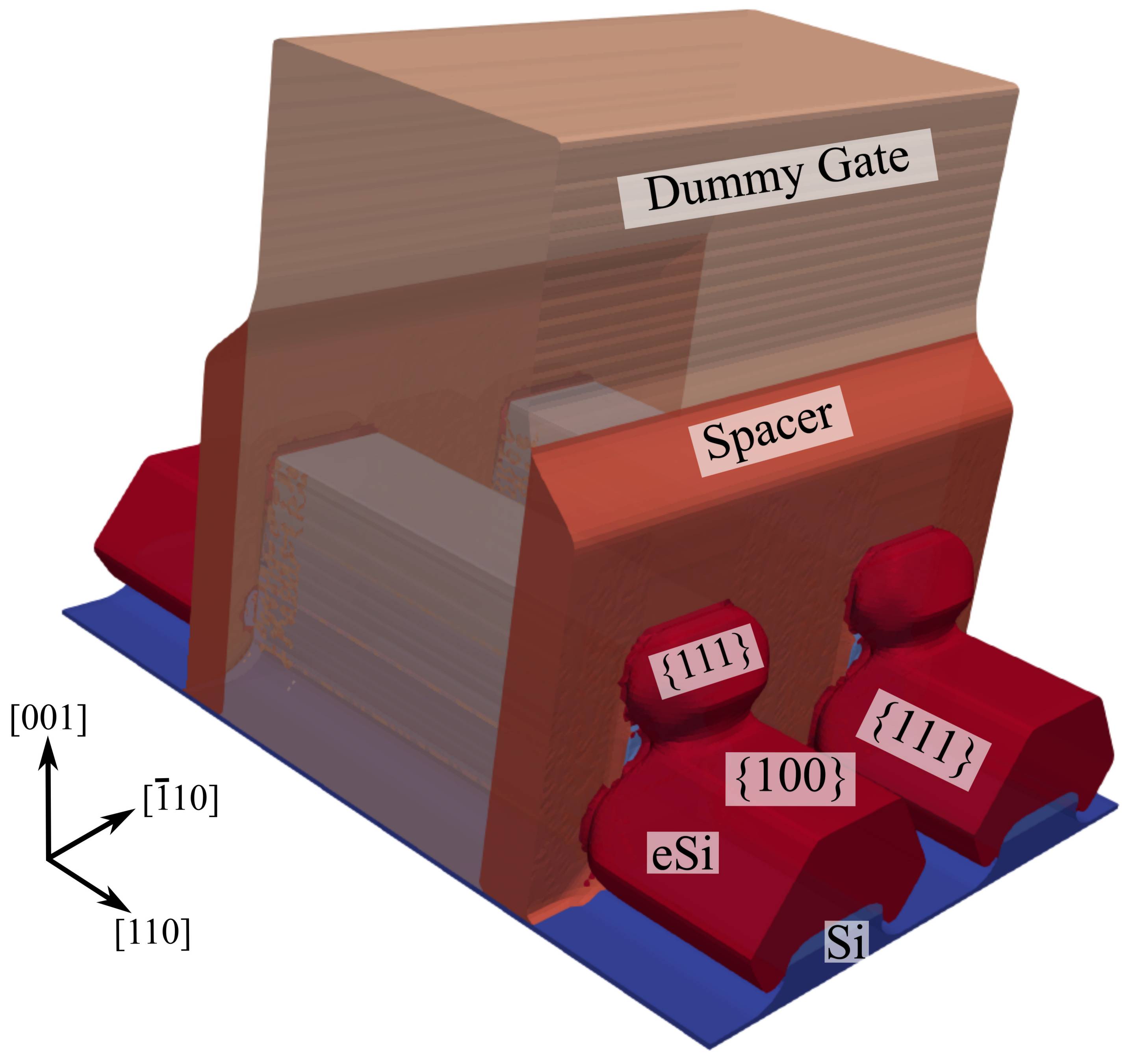
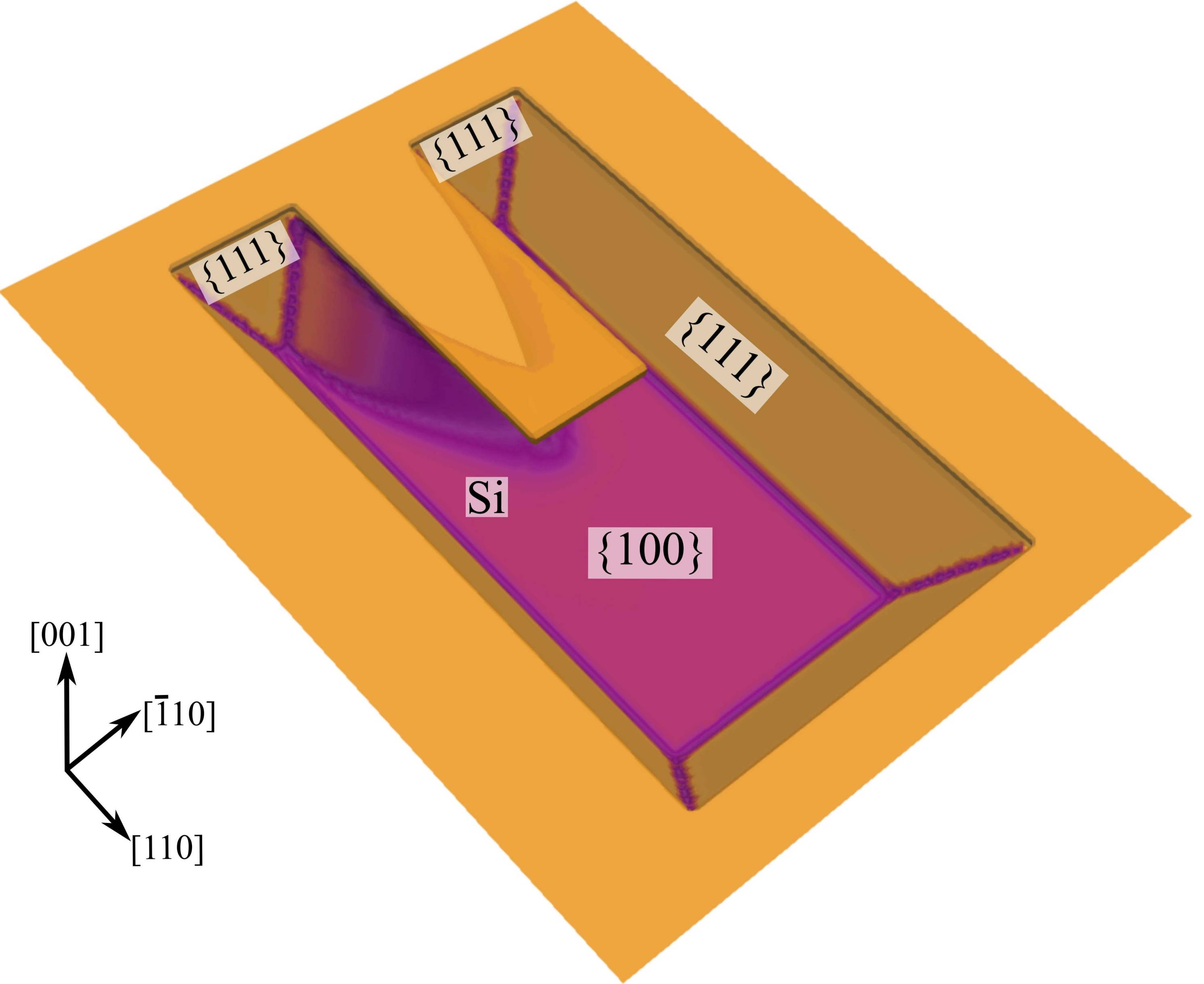
Reprinted with permission from Toifl et al., IEEE Access 8, 115406 [25] (2020). © 2020 Authors, licensed under the Creative Commons Attribution 4.0 License (http://creativecommons.org/licenses/by/4.0/).

Challenges when Modeling Inherently Anisotropic Processes
In the context of process TCAD, inherently anisotropic processes present two main challenges. The first is the choice of an appropriate modeling approach. In general, either macroscopic or microscopic aspects of epitaxial growth
and anisotropic wet etching are studied. Microscopic methods are well-suited for questions regarding the morphology (i.e., microscopic surface features in the sub- range) of semiconductor surfaces. However, the associated high computational effort is a limiting factor. Macroscopic approaches neglect the discrete nature of matter. As a consequence, certain phenomena, such
as crystal defect formation, are not captured. However, simulations of larger systems are enabled, e.g., multi-layered semiconductor devices structures. These approaches are concerned with topography (i.e., geometric features on a
larger, non-atomistic scale), which allows for the application of the level-set method. Furthermore, the modeling approach needs to appropriately incorporate the crystal symmetry of the processed materials.
The second challenge is related to the time evolution of the wafer surface during an inherently anisotropic process. Even though the level-set method has been successfully employed for other semiconductor processes [26]–[32], the strong orientation dependence poses specific challenges. Since orientation-dependence implies sensitivity to the surface geometry (via the local surface normal), an inter-dependency between the surface description and the growth or deposition model emerges. The consequence is that level-set methods for these particular processes are demanding in terms of numerical stability and robustness, even more so if multiple materials are present in the simulation domain [33], [34]. An important requirement for the general applicability of a process simulation is that the surface tracking method does not rely on problem-specific numerical parameters. For the class of inherent anisotropic processes, critical numerical parameters are the dissipation coefficients, which are introduced to stabilize the numerical solution of the level-set equation. Hence, a method to determine these coefficients in a general way is essential to enable reliable and widely applicable selective epitaxy and anisotropic wet etching simulations.
Combining Process and Device TCAD
Naturally, the computational methods developed in process TCAD can be packaged in a software tool, the process simulator, which integrates methods and models for various fabrication processes and thus plays an essential part in semiconductor simulation. By forwarding the process TCAD predicted device geometry to a device simulator, the range of possible scientific and engineering investigations is further broadened. A characteristic example is the patterned substrate of Fig. 1.2: The substrate is utilized as the foundation of gallium nitride (GaN)-based LEDs. A well-known effect in LED design is that the shape of the sapphire substrate significantly impacts the overall efficiency of the LED [35]. Combined process and device TCAD is thus essential to study how process parameters of wet etching (e.g., etchant mixture or temperature) affect the the final device performance. Investigations of this sort are the main motivation for the topography-focused modeling approach presented in this thesis.
1.1 Research Goals
Selective epitaxial growth and anisotropic wet etching are characterized by strongly orientation-dependent growth/etch rates. As a consequence, the semiconductor structures fabricated with these processes exhibit crystal facets contributing to a high complexity of the 3D topography. Computational methods to model these processes are essential to support the 3D design of non-planar semiconductor devices. The research presented in this thesis is thus focused on the following goals.
-
1. Enable stable and robust simulations of 3D selective epitaxial growth and anisotropic wet etching within the context of level-set based process TCAD software frameworks.
-
2. Utilize the simulation methods to simulate the 3D topography of state-of-the-art processing techniques. Provide models to capture the growth and etch evolution of materials with different crystal symmetries and compare the simulation results to experimental observations.
-
3. Study the impact of process parameters (e.g., etch time) on electrical and optical device characteristics by coupling process and device TCAD.
1.2 Research Setting
The research presented in this work was conducted within the scope of the Christian Doppler Laboratory for High Performance TCAD. The Christian Doppler Association funds university-hosted cooperations with companies pursuing joint application-orientated basic research via long-term Laboratory-coined research grants. In this case, the research was lead by Josef Weinbub and involved the Institute for Microelectronics at the TU Wien and Silvaco Inc., a company developing and providing electronic device automation and TCAD software tools.
1.3 Outline of the Thesis
This thesis is structured as follows.
Chapter 2 introduces the fundamental micro- and microscopic phenomena involved in heteroepitaxy and selective epitaxial growth. Various approaches to model epitaxial growth are presented with a special focus on continuum approaches.
The subsequent Chapter 3 follows a similar structure to discuss anisotropic wet etching.
In Chapter 4 numerical schemes for the level-set method, which enable stable and robust simulation of selective epitaxial growth and anisotropic wet etching are derived and assessed. In particular, a novel finite difference Stencil Lax-Friedrichs scheme is introduced, which originates from the viscosity solution of the level-set equations and is based on optimized numerical dissipation coefficients for inherently anisotropic processes. Importantly, the scheme does not require heuristic numerical parameters, which facilitates the practical use. Furthermore, a multi level-set scheme, the deposition top layer method, is proposed to achieve robust selective epitaxy simulations with multiple material regions present in the simulation domain.
In Chapter 5 the numerical schemes are employed to address several state-of-the-art 2D and 3D epitaxy and anisotropic wet etching processes. These stem from various device applications (including MOSFETs, suspended substrates, patterned substrates for LEDs) and cover materials exhibiting different crystal symmetry. Models for these process steps are developed and a procedure to incorporate crystal symmetry is presented. In order to verify the suitability of the modeling approaches, the results are compared with reference experiments from the literature. In particular, a model for anisotropic wet etching sapphire is presented.
This model is further employed in Chapter 6 which focuses on coupling process and device simulation. After discussing the impact of
post-implantation annealing process parameters on silicon carbide (  )-based power device characteristics, the light extraction efficiency of GaN-based LEDs with intricate sapphire topography is investigated.
In the final Chapter 7 a summary and outlook is provided.