

5 Applications
In the previous chapter, the Stencil Lax-Friedrichs scheme and the deposition top layer method were presented. These enable numerically stable level-set simulations of SEG and anisotropic wet etching. In this chapter, these methods are employed to simulate four representative fabrications processes which result in semiconductor structures with complex non-planar topographies:
-
1. Anisotropic wet etching of sigma-cavities which are utilized to fabricate
 MOSFETs with embedded-SiGe (Section 5.1).
-
2. Selective epitaxy of SiGe in oxide trenches, resulting in SiGe fin structures (Section 5.2).
-
3. 3D heteroepitaxy of 3C-SiC1 micro-pillars on
substrates, which is employed to fabricate suspended 3C-SiC substrates (Section 5.3).
-
4. Anisotropic wet etching of sapphire which is utilized for topographical patterning of sapphire substrates and allows for improved GaN-based LEDs (Section 5.4).
In all of these processes characteristic crystal facets emerge, giving rise to complex 2D and 3D topographies. The exact shape of these topographies significantly impact the respective final device, which motivates a continuum
modeling approach. While the processes involving and SiGe result in the common  ,
,  , and
, and  facets encountered in the previous chapters, the 3C-SiC micro-pillars and the sapphire substrates display a broader range of crystal facets. This is due to the tetrahedral crystal symmetry of 3C-SiC and trigonal symmetry
of sapphire, respectively, which is in contrast to the octahedral symmetry associated with and SiGe. Furthermore, experimental studies have been performed in the literature for all four process applications. Hence, experimentally characterized topography profiles are available and enable the evaluation of the
simulation approach.
facets encountered in the previous chapters, the 3C-SiC micro-pillars and the sapphire substrates display a broader range of crystal facets. This is due to the tetrahedral crystal symmetry of 3C-SiC and trigonal symmetry
of sapphire, respectively, which is in contrast to the octahedral symmetry associated with and SiGe. Furthermore, experimental studies have been performed in the literature for all four process applications. Hence, experimentally characterized topography profiles are available and enable the evaluation of the
simulation approach.
In order to simulate the topography evolution with the level-set method, physics-based models expressed with a velocity function  , are required. The four processes discussed in this chapter have orientation-dependent growth/etch rates, which imply a velocity function that solely depends on the direction of the local surface normal
  . Hence, each process is associated with a velocity function
  . Usually only a limited number of rates is known from experiments. However, since a continuous is required for the level-set method, growth/etch rates have to be provided for every possible surface normal . Thus, an interpolation scheme is necessary. However, the interpolation must respect the crystal symmetry. In the case of octahedral symmetry associated with and SiGe, an interpolation method proposed by Hubbard [145] has been established as the
standard procedure [99]. However, Hubbard interpolation cannot be applied for tetrahedral and trigonal symmetry. Hence, alternative
techniques are required, which motivates the introduction of a generalized symmetry-respecting interpolation approach in this chapter (Section 5.3.1).
. Usually only a limited number of rates is known from experiments. However, since a continuous is required for the level-set method, growth/etch rates have to be provided for every possible surface normal . Thus, an interpolation scheme is necessary. However, the interpolation must respect the crystal symmetry. In the case of octahedral symmetry associated with and SiGe, an interpolation method proposed by Hubbard [145] has been established as the
standard procedure [99]. However, Hubbard interpolation cannot be applied for tetrahedral and trigonal symmetry. Hence, alternative
techniques are required, which motivates the introduction of a generalized symmetry-respecting interpolation approach in this chapter (Section 5.3.1).
The individual processes presented here are part of a process sequence to fabricate a specific device. In order to focus on SEG and anisotropic wet etching steps, all other steps, such as dry etching, are not modeled with physics-based models. Instead, geometric process emulation is employed: The topography resulting from these fabrication processes are replicated, using purely geometric surface propagation, i.e., ideal profile evolution based on geometric quantities (e.g., film thickness). This approach allows to produce the exact initial topography for the subsequent SEG or anisotropic wet etching step. Hence, the assessment of the capability of the level-set continuum models for the four anisotropic processes is enabled. In all cases, the simulation results are compared with experimental observations, which allows for verification of the simulation methodology.
In this chapter, the continuum modeling of the four processes given at the outset is presented. The discussion proceeds in the following structure: First, the respective process application is introduced and the significance of the SEG or anisotropic wet etching process for the final device is discussed. Second, the modeling and interpolation methods are presented. Third, the resulting level-set continuum model is applied to simulate the process step and compare the simulation results with experimental observations from the literature.
1 3C-SiC is a cubic polytype of silicon carbide (SiC), i.e., a form of SiC, which crystallizes in the Zincblende structure [40].
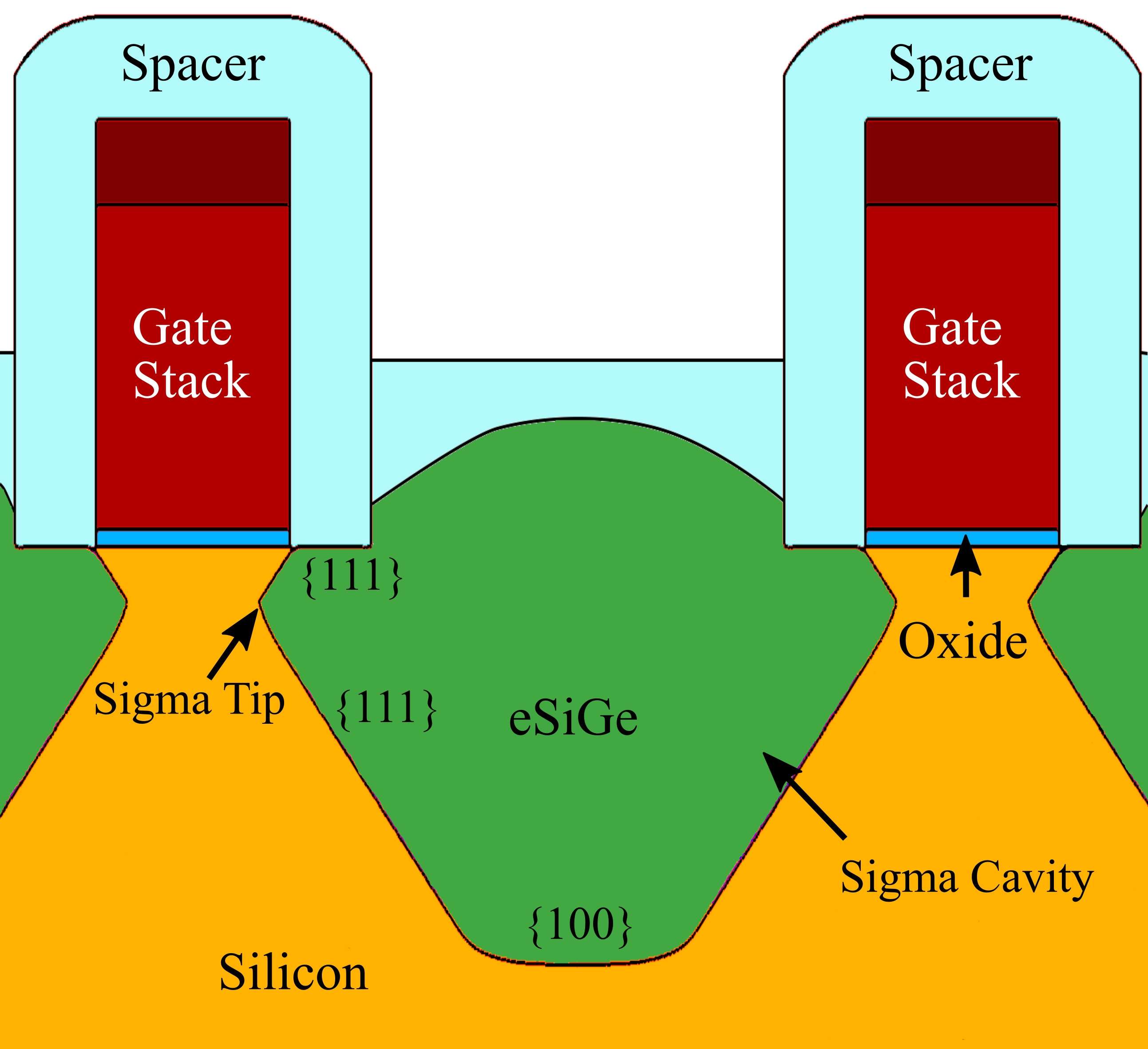
5.1 Sigma-Cavity for Embedded-SiGe MOSFETs
Anisotropic wet etching is widely associated with processing of structures in the micrometer scale (MEMS). However, there are also applications on the nanoscale. One of them is the technology of embedded silicon germanium
(eSiGe), present in source/drain (S/D) engineering of MOSFETs. The anisotropic etchant TMAH is typically employed to produce sigma-cavities with precise geometric requirements, which are subsequently filled with eSiGe [146]. Fig. 5.1 illustrates the typical structure of a S/D
engineered planar p-channel MOSFET. In order to fabricate sigma-cavities, a combination of dry and anisotropic wet etching is employed. A RIE process produces the initial profile for a subsequent anisotropic wet etching step with
TMAH. Due to the slowly etching planes, the final etch profile consists of sharp corners defined by these planes at specific positions relative to the channel (sigma-cavity tip). The position of the sharp corners is an essential design consideration, which is
expressed in terms of the design parameters tip depth and channel-cavity distance. These parameters have a significant impact on the exact magnitude of compressive stress in the channel induced by the subsequently grown
eSiGe [147]. Compressive stress improves the carrier mobility and thus allows to realize higher drain currents in
the final MOSFET for a given gate voltage [148].
In this section, the sigma-cavity etching for sub-28 nm source/drain (S/D) engineered p-channel MOSFET, as experimentally demonstrated by Qin et al. [147], is considered. A model for the etch rate distribution function is constructed. On that account, an interpolation scheme which reflects the symmetry of the etch anisotropy is discussed. The calibrated model is then used to simulate the etch profile evolution and the results are
compared with experimental profiles obtained from scanning electron microscopy (SEM).
5.1.1 Hubbard Interpolation for Octahedral Symmetry
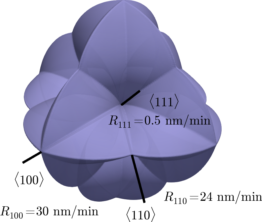
When etching with TMAH, the essential crystal facets observed in experiments are ,  , and , as discussed in Section 3.1. The associated etch rates are typically available with high accuracy and appropriately characterize the etch
rate anisotropy (which is justified by the reaction-limited nature of anisotropic wet etching, as discussed in Section 3.2.2). In order to employ
in the level-set method, an etch rate must be available for every possible direction on the unit sphere
, and , as discussed in Section 3.1. The associated etch rates are typically available with high accuracy and appropriately characterize the etch
rate anisotropy (which is justified by the reaction-limited nature of anisotropic wet etching, as discussed in Section 3.2.2). In order to employ
in the level-set method, an etch rate must be available for every possible direction on the unit sphere

Hence, an interpolation scheme to determine the entire distribution from the characteristic etch rates is required. The standard approach is an interpolation method introduced by Hubbard [145] (Hubbard interpolation). is a highly symmetrical crystal with the associated octahedral crystallographic point group (Schoenflies notation  ). A crystallographic point group characterizes the set of symmetry operations that leave the crystal structure unchanged [41]. Octahedral symmetry involves 48 symmetry operations, which provides the possibility to only consider a subset of the unit sphere
  and still have a complete picture of the etch anisotropy.
  is
is  -th of the unit sphere in the traditional Hubbard interpolation, as shown in Fig. 5.2. Interpolation between experimental etch rates , , , and (if desired) is performed on by applying trilinear interpolation between the nearest supporting values. With the help of the symmetry operations the interpolated values on are associated with the entire unit sphere
  and thus a fully-defined is constructed.
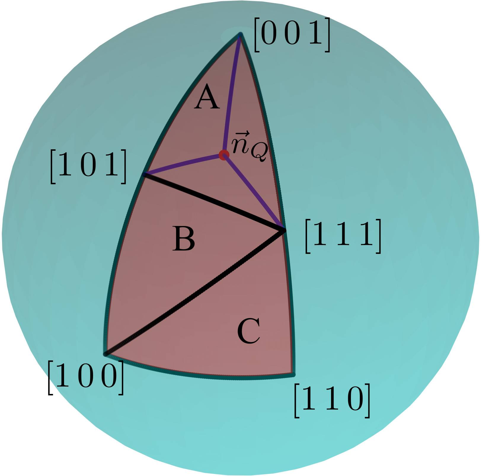
 the unit sphere is reduced to of the sphere. (a) Three-rate interpolation setup ( , , ). A general surface normal vector is first mapped to the crystallographically equivalent
  . Depending on the orientation, the interpolation supporting values of the respective triangle are used to calculate
  with trilinear interpolation. (b) Four-rate interpolation setup including .
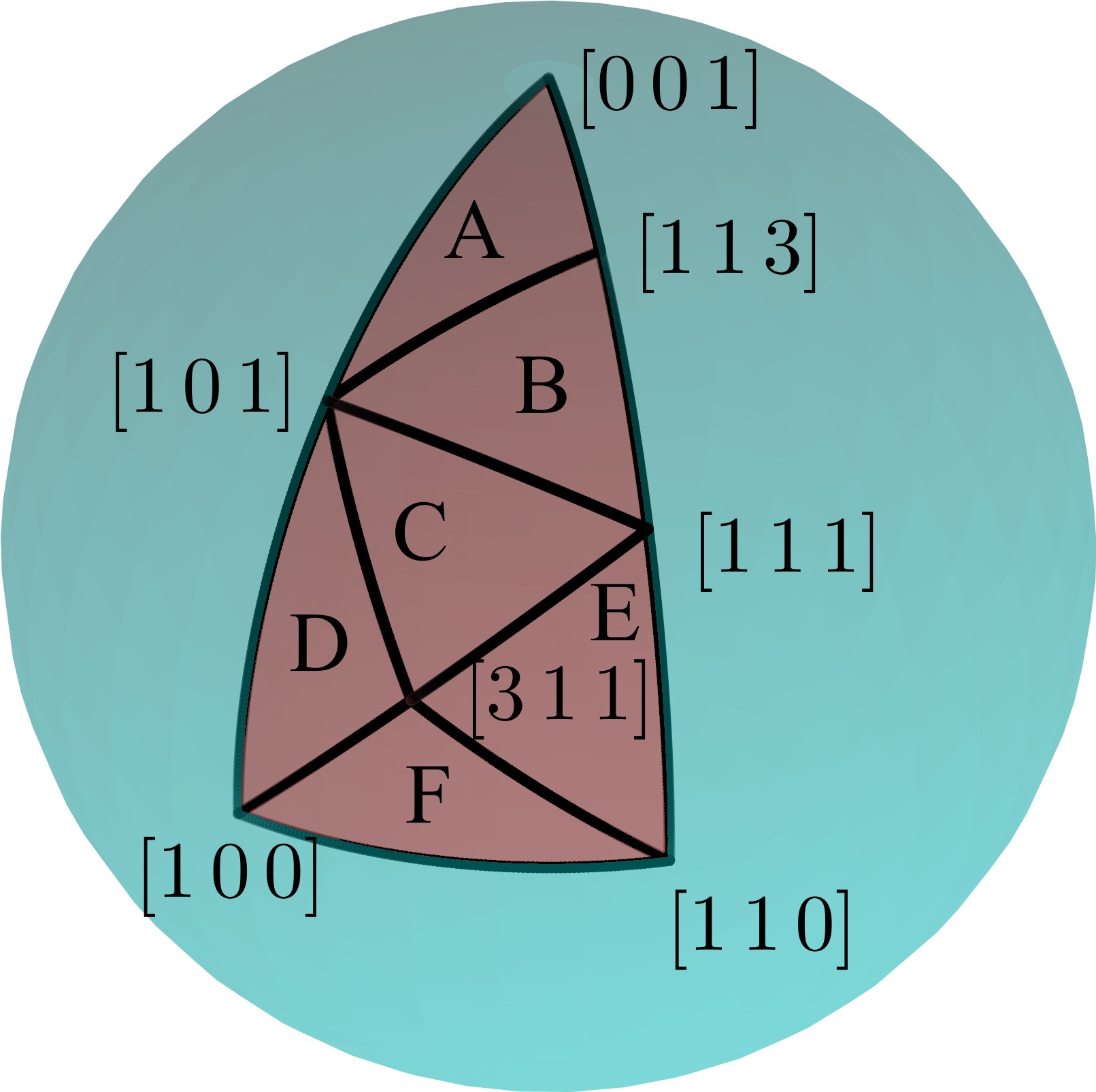
As pointed out in Section 3.2.2, for some applications high-index crystal facets are particularly important and thus desired to be well-resolved in
simulations. The Hubbard interpolation can be extended by incorporating more crystal directions, which can be achieved by including more triangles in the partitioning of . With more experimental rates, high-order interpolation schemes and multiple options for triangulation are available. The optimal triangulation and interpolation technique depends on the Miller indices of experimentally
available directions and associated etch rates, as shown in a study by Gosálvez et al. [99]. However, for many applications involving anisotropic wet etching of trilinear Hubbard interpolation is sufficient.
Due to the high symmetry of , the Hubbard interpolation approach can also be expressed as an analytical function with case differentiation [33], [118]. Analytical functions are straightforwardly implemented in a level-set tool and
thus enable efficient evaluation of during surface propagation. However, it is important to note that the ability to find analytic expressions is facilitated by the extraordinary high symmetry of the crystal. In less symmetric crystals, more general schemes are required, which is further discussed in Section 5.3.1 and Section 5.4.1.
5.1.2 Modeling and Results

 for all unit vectors . (b) Stereographic projection, as defined in (5.2).
Reprinted with permission from Toifl et al., Proc. Int. Conf. Simulation Semiconductor Processes Devices (SISPAD) (2019), pp. 327-330 [149], © 2019 IEEE.
The anisotropic wet etch step in the sigma-cavity process, as presented by Qin et al. [147], is performed with a TMAH solution of
2.38 wt% at 40 °C. The etch process is stopped after 30 s. The etching anisotropy of Si with the TMAH is modeled using three-rate Hubbard interpolation. The interpolation supporting values are
 ,
,  , and
, and  .
.  has been measured by Qin et al. and
  can be directly deduced from the published SEM images. Furthermore,
  is a calibration parameter which is chosen in accordance with similar TMAH solutions from the literature [100], [101]. The resulting interpolated etch distribution is depicted in Fig. 5.3, where a 3D plot and a heatmap of a stereographic projection plot are used to visualize the spatial distribution. The stereographic projection is
centered at the south pole
is a calibration parameter which is chosen in accordance with similar TMAH solutions from the literature [100], [101]. The resulting interpolated etch distribution is depicted in Fig. 5.3, where a 3D plot and a heatmap of a stereographic projection plot are used to visualize the spatial distribution. The stereographic projection is
centered at the south pole  and maps points on the unit sphere
  onto a plane with

Fig. 5.3b shows the projection for points with  (northern hemisphere), which results in a circular image. In particular, trilinear Hubbard interpolation between
  ,
,  , and
, and  is elegantly visualized in a stereographic projection.
The fabrication of the sigma-cavities is simulated using Silvaco’s Victory Process simulator [140], [149], where the proposed CA engine (4.36) has been incorporated into a narrow band level-set engine. Fig. 5.4a shows the time evolution of the simulation. First, the gate stack and spacer geometry is emulated by geometric deposition techniques. In order to focus on the investigation of the wet etching process, the topography induced by a two-step RIE process is replicated by an ideal anisotropic and isotropic dry etching step (Fig. 5.4b). Thus, it is ensured that the post-dry etch profile coincides exactly with the experimentally observed reference. The subsequent anisotropic wet etching simulation is performed with the stabilizing Stencil Lax-Friedrichs scheme.

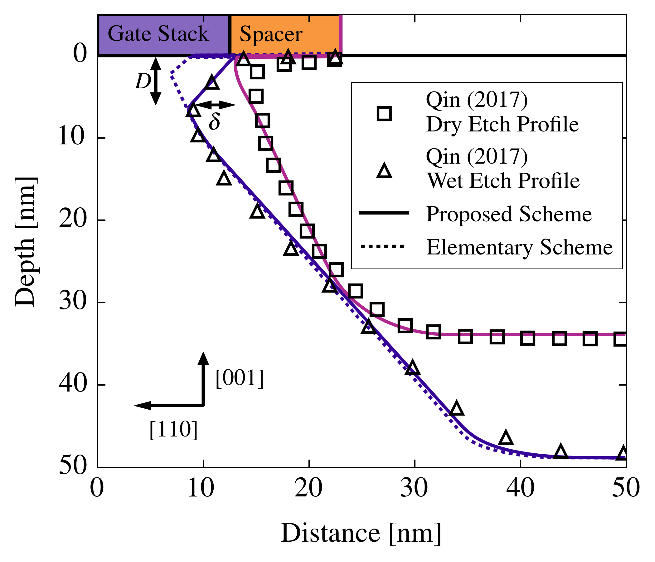 planes. (b) Comparison of the simulation results with the experimental profiles characterized by Qin et al. [147].
The sigma tip position is accurately resolved with the Stencil Lax-Friedrichs scheme (indicated as proposed scheme), while the elementary scheme (4.19)
results in an error of 1.6 nm in x-direction and 4.2 nm in y-direction. The spatial resolution is
planes. (b) Comparison of the simulation results with the experimental profiles characterized by Qin et al. [147].
The sigma tip position is accurately resolved with the Stencil Lax-Friedrichs scheme (indicated as proposed scheme), while the elementary scheme (4.19)
results in an error of 1.6 nm in x-direction and 4.2 nm in y-direction. The spatial resolution is  .
.Reprinted with permission from Toifl et al., Proc. Int. Conf. Simulation Semiconductor Processes Devices (SISPAD) (2019), pp. 327-330 [149], © 2019 IEEE.
During all calculations the level-set equation is discretized on a regular grid with a spatial resolution  and the level-set narrow band is defined by
  . Fig. 5.4a illustrates the time evolution to the final etch profile. The initial post-RIE profile and the wet etch profile after
  ,
,  , and
, and  , respectively, are shown. During the etching process the characteristic facets are formed and subsequently define the etch profile. The design parameters tip depth
  and channel-cavity distance
  are depicted in Fig. 5.4b. The simulation results are compared with experimentally obtained etch profiles presented by Qin et al. [147]. Most importantly, , , and the cavity depth are accurately reproduced by the simulation.
In order to assess the influence of the CA engine in practical applications, the same process simulation steps are performed with the elementary dissipation coefficients (4.19). As shown in Fig. 5.4b, the elementary
dissipation coefficients are insufficient to stabilize the front propagation. This results in artificially high undercut rate and thus causes the prediction of incorrect sigma tip position. Compared to experimental observations, the sigma
tip position is displaced by 1.6 nm in x-direction and 4.2 nm in y-direction, which is an unacceptable error given the spatial resolution . The Stencil Lax-Friedrichs scheme (4.36) proposed in this thesis, however, is capable of
reproducing the physical undercut and thus predicting the geometry of the sigma-shaped cavity with high accuracy.
The sigma-cavity process demonstrates the capability of the stabilization scheme in practical simulations of anisotropic wet etching processes. In the next section, the focus is shifted to an application of Stencil Lax-Friedrichs scheme for SEG of SiGe.
5.2 Selective Epitaxy of SiGe
SEG of SiGe is employed in various fabrication processes. A typical growth process, as employed to fabricate S/D engineered fin FETs, has already been shown in Fig. 1.5. In
this section a further application is discussed: Selective heteroepitaxy of SiGe fins in trench arrays. The main motivation to grow SiGe crystals on substrates is to enhance carrier mobility in the transistor channel by means of introducing strain with SiGe layers [150]. In particular, SiGe crystals are used as source/drain stressors to improve hole mobility in p-type FETs [24]. The strain is induced by the hetero-interface between the SiGe film and substrate, as indicated in (2.6). Here, SiGe refers to the set of alloys  , where the fraction of
  (
(  ) depends on the growth conditions. However, as discussed in Section 2.1.5, the lattice mismatch at the hetero-interface
results in defects which degrade device performance. One approach to decrease defect density in the epitaxial layer is aspect ratio trapping. In narrow oxide trenches defects are trapped at oxide sidewalls [151], which motivates the usage of trench structures.
) depends on the growth conditions. However, as discussed in Section 2.1.5, the lattice mismatch at the hetero-interface
results in defects which degrade device performance. One approach to decrease defect density in the epitaxial layer is aspect ratio trapping. In narrow oxide trenches defects are trapped at oxide sidewalls [151], which motivates the usage of trench structures.
The topography of selectively grown SiGe layers plays an important role for the global strain distribution in the epitaxial layer and also for parasitic capacitances and resistances in the final device. Thus, it is important to account
for the geometric shapes formed by the characteristic facets ( , , , and ). Since typical SEG processes proceed close to stationary kinetic growth (Section 2.1.4), the CA engine can be employed
with growth distributions .
In an experimental setup presented by Jang et al. [52] epitaxial SiGe fins with high crystal
quality are selectively grown. This is achieved by first thermally oxidizing  substrates, which are subsequently patterned with dry etching to fabricate trenches aligned along
 ![\( \left [ \overline {1}\, 1 \, 0 \right ] \)](PhD_Thesis-images/13BF96C07980AF8FCA57A29D070B8651.svg) . Due to the non-zero dry etch rate of , also grooves in the substrate are formed. Epitaxy is performed in an ultra-high vacuum CVD reactor (pressure
. Due to the non-zero dry etch rate of , also grooves in the substrate are formed. Epitaxy is performed in an ultra-high vacuum CVD reactor (pressure  ) at
) at  . Fig. 5.5 shows a visualization of the final topography. The SEG process is based on a cyclic procedure (see also Section 2.1.5). After initial isotropic etching with diluted hydrofluoric acid to remove native
  , the following processes are repeated:
-
• 15 s deposition from flowing source gas
 and
and  . The flow rate of is fixed with 20 sccm (cubic centimeters per minute under standard conditions for temperature and pressure), while the rate of depends on desired composition and is in the range from 50 sscm to 200 sscm.
-
• 12 s etch with
 , where nucleated
  on is removed.
Jang et al. [52] published plain wafer deposition rates and SEM and high-resolution transmission electron microscopy (TEM) images for several alloys. These measurements provide the reference for the modeling approach.
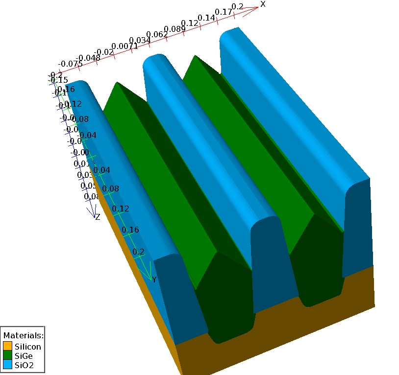
sidewalls.
Modeling and Results
In order to model the SEG process, the cyclic process is abstracted to a continuous epitaxy process that is perfectly selective, i.e., the deposition rate on oxide regions is 0. In the experimental study [52], deposition rates have been measured for , , and facets. Since it is a cyclic process the rates have been reported in units of nm/cycle. These rates are used as supporting values for the four-rate Hubbard interpolation of the deposition rate distribution (cf. Section 5.1.1) and are given in Tab. 5.1. The CA engine proposed in this thesis
(and implemented in Silvaco Victory Process) is employed to simulate the epitaxial growth. In particular, the deposition top layer is enabled and a regular Cartesian grid with ![\( \Delta x = \SI [round-precision=3]{0.002}{\micro \meter } \)](PhD_Thesis-images/8C3C62E507ACD6D092DE09797EC13FE4.svg) is used. The initial dry-etching step is emulated with geometric process steps, in order to realize the exact experimental shape of the initial sidewalls and grooves.
is used. The initial dry-etching step is emulated with geometric process steps, in order to realize the exact experimental shape of the initial sidewalls and grooves.
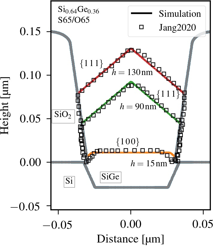
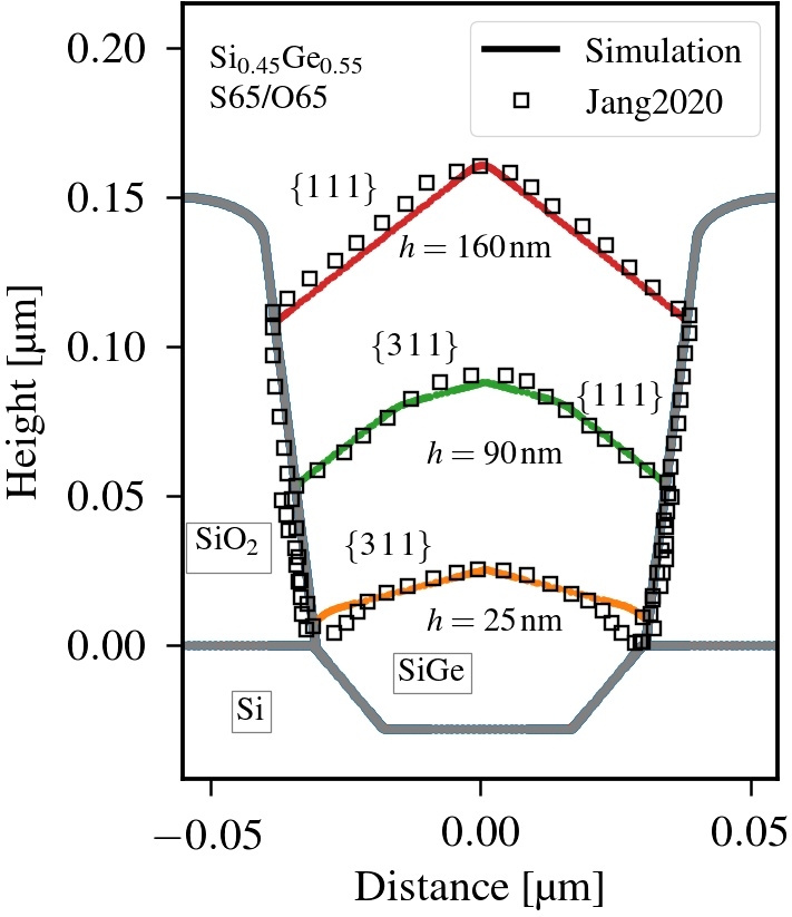
The simulation results are compared with cross-sectional TEM images presented for SiGe alloys  and
and  [52]. For both alloys the time evolution of the epitaxial growth is illustrated by three TEM images
representing the SiGe crystal at certain heights
[52]. For both alloys the time evolution of the epitaxial growth is illustrated by three TEM images
representing the SiGe crystal at certain heights  . The corresponding cross-sectional profiles are referred to as
  ,
,  , and
, and  in the following. Fig. 5.6a and Fig. 5.6b show the comparison of the simulation results with the
experiments. Since the rates are given in units of nm/cycle, the time variable is given by the number of deposition and subsequent etch cycles. The experimental TEM images with SiGe crystals at height correspond to a certain number of cycles as indicated in Tab. 5.1.
in the following. Fig. 5.6a and Fig. 5.6b show the comparison of the simulation results with the
experiments. Since the rates are given in units of nm/cycle, the time variable is given by the number of deposition and subsequent etch cycles. The experimental TEM images with SiGe crystals at height correspond to a certain number of cycles as indicated in Tab. 5.1.
Caused by the relative difference in net deposition rates, the alloys and show different topography evolutions. As shown in Fig. 5.6b, facets dominate the growth as soon as the small cavity is completely filled. Similar to the wet etching case in Section 5.1, the rates associated with are global minima of . Even though this is also the case for higher concentration, the apparent difference is the appearance of facets. This can be explained with the rate ratio  , which is
  (
(  ) for
) for  ( ). Since the ratio is larger for the higher concentration, the growth proceeds longer before dominates the topography. Furthermore, deviations from the experimental results can be observed in the early stages ( ) of growth. These can be attributed to the assumption of negligible surface diffusion which is inherent in a model (cf. Section 2.1). Nevertheless, the excellent agreement of simulation and experimental results demonstrates the
robustness, stability, and capability of CA engine based continuum modeling of SEG.
( ). Since the ratio is larger for the higher concentration, the growth proceeds longer before dominates the topography. Furthermore, deviations from the experimental results can be observed in the early stages ( ) of growth. These can be attributed to the assumption of negligible surface diffusion which is inherent in a model (cf. Section 2.1). Nevertheless, the excellent agreement of simulation and experimental results demonstrates the
robustness, stability, and capability of CA engine based continuum modeling of SEG.
,  , and have been adopted from the presented measurements [52]. The number of deposition cycles
  indicate how many SEG cycles are required to achieve the topographies which have been provided with TEM images (the respective profiles are given in Fig. 5.6).
| Rates [nm/cycle] |
|
||||||||
| Ge [%] | |
|
|
|
|
 |
 |
||
| 36 | 5 | 3 | 3.5 | 1 | 8 | 33 | 55 | ||
| 55 | 13 | 5 | 3.1 | 1.6 | 5 | 24 | 47 | ||
In the following section the 3D heteroepitaxy of 3C-SiC on substrates is discussed, which is characterized by emerging crystal facets with tetrahedral symmetry.
5.3 Heteroepitaxy of 3C-SiC on Si(111) Micro-Pillars
Aside from SEG, the level-set method can also be applied to simulate heteroepitaxy in growth conditions which are far from thermal equilibrium. As discussed in Section 2.2.5, a model of kinetic crystal growth can be successfully employed to capture the essentials of the growth evolution in certain
configurations. In this section, the heteroepitaxy of 3C-SiC on pre-patterned micro-pillars is considered. This fabrication process is motivated by the idea of using 3C-SiC as substrate for  -based power devices in the voltage rage from 600 V to 1200 V 2. In general, SiC substrates are comparatively expensive to fabricate. Potentially
cheaper substrates can be fabricated by growing 3C-SiC on industry-standard substrates. However, it is difficult to achieve thick 3C-SiC layers with high crystalline quality (i.e., monocrystalline and low defect density). Direct deposition on Si wafers is only feasible for thin layers, because of the large
misfit between the lattice parameters and thermal expansion coefficients. As a result, stacking faults and wafer bowing are caused [152]. One possibility to improve the film quality is to grow a 3C-SiC film in a suspended way on top of micrometer-sized pillars. In such a configuration, strain can be (plastically) relieved by pillar tilting and rotation [153]. As the growth continues, individual 3C-SiC crystals ultimately coalesce and form a high-quality suspended 3C-SiC substrate.
-based power devices in the voltage rage from 600 V to 1200 V 2. In general, SiC substrates are comparatively expensive to fabricate. Potentially
cheaper substrates can be fabricated by growing 3C-SiC on industry-standard substrates. However, it is difficult to achieve thick 3C-SiC layers with high crystalline quality (i.e., monocrystalline and low defect density). Direct deposition on Si wafers is only feasible for thin layers, because of the large
misfit between the lattice parameters and thermal expansion coefficients. As a result, stacking faults and wafer bowing are caused [152]. One possibility to improve the film quality is to grow a 3C-SiC film in a suspended way on top of micrometer-sized pillars. In such a configuration, strain can be (plastically) relieved by pillar tilting and rotation [153]. As the growth continues, individual 3C-SiC crystals ultimately coalesce and form a high-quality suspended 3C-SiC substrate.
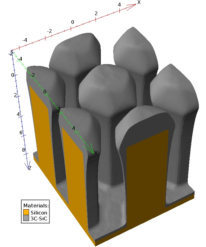
In a process presented by Kreilinger et al. [154], a  substrate is patterned with deep reactive ion etching (DRIE) to fabricate arrays of pillars. substrates are used, because the similar lattice structure allows for the best possible defect reduction. The -pillars are arranged in a hexagonal pattern which is illustrated in Fig. 5.7. Subsequently, 3C-SiC is epitaxially grown in a horizontal CVD reactor in the
low-pressure regime (100 mbar) at 1370 °C. The precursors are
substrate is patterned with deep reactive ion etching (DRIE) to fabricate arrays of pillars. substrates are used, because the similar lattice structure allows for the best possible defect reduction. The -pillars are arranged in a hexagonal pattern which is illustrated in Fig. 5.7. Subsequently, 3C-SiC is epitaxially grown in a horizontal CVD reactor in the
low-pressure regime (100 mbar) at 1370 °C. The precursors are  and trichlorosilane. This process has been considered in a simulation study [83], where a Cahn
Taylor phase-field model (Section 2.2.5) has been employed. In the following, an alternative approach using the level-set method
with a growth distribution is demonstrated.
and trichlorosilane. This process has been considered in a simulation study [83], where a Cahn
Taylor phase-field model (Section 2.2.5) has been employed. In the following, an alternative approach using the level-set method
with a growth distribution is demonstrated.
In order to appropriately construct , it is important to ensure that the symmetry of 3C-SiC is respected. Contrary to the octahedral symmetry of , the crystal facets observed during epitaxial growth of 3C-SiC reflect the Zincblende structure of the crystal [155]. For instance, ![\( \left [1\,\overline {1}\,1\right ] \)](PhD_Thesis-images/72D2FEC2DD190F85B0B8BABEFE42B2BB.svg) facets do not grow with the same etch rate as
facets do not grow with the same etch rate as ![\( \left [1\,1\,1\right ] \)](PhD_Thesis-images/A7BBC5D80D994A7ABB5641BB394489FC.svg) , a fact which is often expresses by the distinction of
, a fact which is often expresses by the distinction of  (Si-terminated) and
  (C-terminated) facets [83]. As a consequence, Hubbard interpolation cannot be employed to
construct . A more general approach to account for crystal symmetry is presented in the next section and applied to the case of 3C-SiC.
(C-terminated) facets [83]. As a consequence, Hubbard interpolation cannot be employed to
construct . A more general approach to account for crystal symmetry is presented in the next section and applied to the case of 3C-SiC.
2  -based devices typically target higher voltage ranges [40].
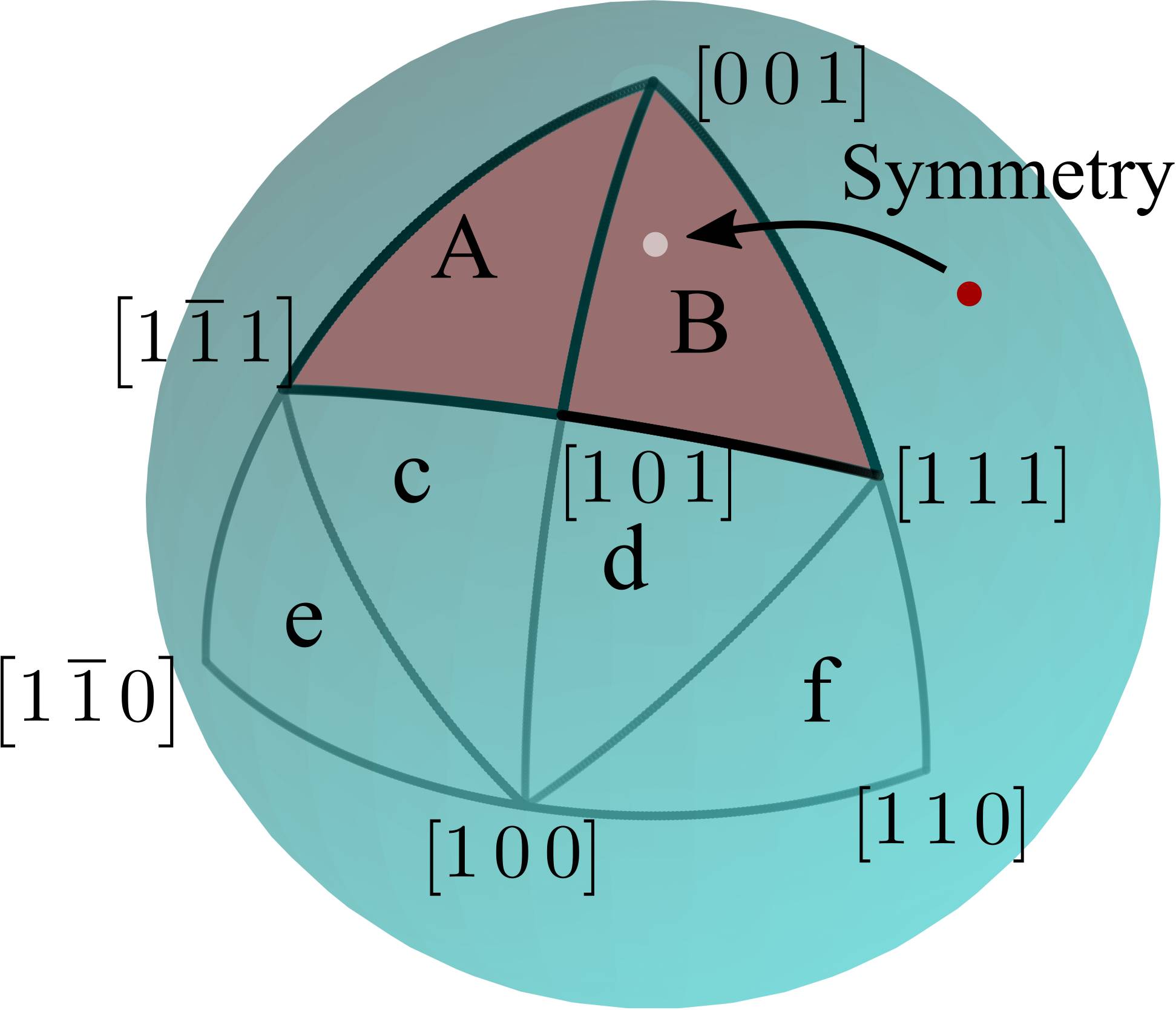
5.3.1 Growth Rates in Tetrahedral Symmetry

, tetrahedral  , and ditrigonal scalenohedral symmetry
  ). The operations involve rotation and rotation-reflections and are displayed in stereographic projection [41],
[156].
). The operations involve rotation and rotation-reflections and are displayed in stereographic projection [41],
[156].
The ideas of Hubbard interpolation, as presented in Section 5.1.1, can be generalized to enable interpolation of growth rates in non-octahedral symmetry. Every
crystal symmetry is associated with a point group which defines the set of symmetry operations that map a crystal direction to another crystallographically equivalent direction  . Fig. 5.8 depicts a commonly used visualization of symmetry operations on the basis of stereographic plots (cf. (5.2)). Three different point groups are shown and designated in Schönflies notation [41], [156], which is a system to uniquely classify point groups. As evident from the
number of operations, the octahedral group has a higher degree of symmetry than the tetrahedral group , which is the point group associated with the Zincblende structure.
. Fig. 5.8 depicts a commonly used visualization of symmetry operations on the basis of stereographic plots (cf. (5.2)). Three different point groups are shown and designated in Schönflies notation [41], [156], which is a system to uniquely classify point groups. As evident from the
number of operations, the octahedral group has a higher degree of symmetry than the tetrahedral group , which is the point group associated with the Zincblende structure.
There is an important property associated with the set of symmetry operations. For every point group, a special subset of the unit sphere  exists, which is the smallest subset that contains all crystallographically equivalent directions.
  is referred to as fundamental domain and has the property of getting smaller with larger number of symmetry operations. In order to construct , it is sufficient to perform interpolation only on . This can be practically achieved by mapping every direction
  to the respective direction in the fundamental domain
  , a process which is referred to as reduction to the fundamental domain in the following. Since the entire can also be subjected to symmetry operations, the location of is not unique. As a consequence, a specific location can be suitably chosen to simplify the involved rotations and reflection operations.
point group and auxiliary spherical triangles, which are used in the algorithm to reduce crystal directions to the fundamental domain (Fig. 5.10).
The construction of symmetry-respecting function is thus a three-step process:
-
1. Identify the point group associated with growth/etch anisotropy and choose one instance of the fundamental domain
.
-
2. Apply an algorithm which maps every input vector
to by only using symmetry operations.
-
3. Perform interpolation on
based on interpolation supporting values (i.e., characteristic directions).
This procedure is generally applicable for every possible crystal symmetry. In special cases, a subset of the unit  which is larger that can be utilized to computationally optimize certain sub steps. For instance, the computation of symmetry operations in step 2 might be simpler on a larger subset, as it is the case in the Hubbard interpolation
method.
which is larger that can be utilized to computationally optimize certain sub steps. For instance, the computation of symmetry operations in step 2 might be simpler on a larger subset, as it is the case in the Hubbard interpolation
method.

(input) to the crystallographically equivalent direction residing in the fundamental domain  (output). The superscript
  refers to the vector representation in spherical coordinates with polar angle
  and azimuthal angle
  .
.  denotes two-fold rotation about
 ![\( \left [1\,0\,0\right ] \)](PhD_Thesis-images/AB02DF5E12FF156B4FA9A6A453B3A07B.svg) and
and  indicates three-fold rotation about . Reflection in a plane is indicated as
  , where
  and
and  . Lowercase letters denote the auxiliary spherical triangles visualized in Fig. 5.9.
The fundamental domain of tetrahedral symmetry is illustrated in Fig. 5.9 with red color on the unit sphere. forms a spherical triangle with vertices , , and ![\( \left [0\,0\,1\right ] \)](PhD_Thesis-images/FB1585927809A07A2B8E678E8B8A9D5A.svg) and can be divided into two smaller spherical triangles with the additional vertex
and can be divided into two smaller spherical triangles with the additional vertex ![\( \left [1\,0\,1\right ] \)](PhD_Thesis-images/11C0D329AD68CD1D05F14CF8284574F7.svg) . These are labeled A and B in Fig. 5.9. Furthermore, four additional spherical triangles (gray edges) are shown and labeled with lower case letters (c, d, e, and f).
These are of importance in the algorithm to reduce a general input unit vector to .
. These are labeled A and B in Fig. 5.9. Furthermore, four additional spherical triangles (gray edges) are shown and labeled with lower case letters (c, d, e, and f).
These are of importance in the algorithm to reduce a general input unit vector to .
The idea of this algorithm is, in a first step, to apply symmetry operations to transport to the large spherical triangle which is shown in Fig. 5.9 and has vertices , ![\( \left [1\,\overline {1}\,0\right ] \)](PhD_Thesis-images/D51491CF454A9F70D9C6BD244B05F176.svg) , and
, and ![\( \left [1\,1\,0\right ] \)](PhD_Thesis-images/0B0A9331779FAA18693BD3B73523539E.svg) . In a second step, all directions outside are subjected to crystal operations depending on the spherical triangle (c, d, e, or f) they have been transferred to. The algorithm is visualized in a flow chart in Fig. 5.10 and uses the following symmetry operations:
. In a second step, all directions outside are subjected to crystal operations depending on the spherical triangle (c, d, e, or f) they have been transferred to. The algorithm is visualized in a flow chart in Fig. 5.10 and uses the following symmetry operations:
-
• Two-fold rotation about
, notated as .
-
• Three-fold rotation about
, notated as . Can also be applied two times in succession, then notated as  .
.
-
• Reflection in a plane, notated as
with , .
Interpolation on is performed with supporting values for , , and . Depending on the location of , i.e.,  or
or  , the respective vertices are used. The interpolation on spherical triangles with vertices
  is based on spherical barycentric coordinates, which are given by [157]

with
![(5.5–5.6) \{begin}{align} \label {eq:bary_2} \vec {K}_1 &= \left [\vec {n}_\mathrm {F} \cdot (\vec {v}_2 \times \vec {v}_3), \vec {n}_\mathrm {F} \cdot (\vec {v}_3 \times \vec
{v}_1), \vec {n}_\mathrm {F} \cdot (\vec {v}_1 \times \vec {v}_2)\right ]^\intercal ,\\ \vec {K}_2 &= \left [\vec {v}_1 \cdot (\vec {v}_2 \times \vec {v}_3), \vec {v}_2 \cdot (\vec {v}_3
\times \vec {v}_1), \vec {v}_3 \cdot (\vec {v}_1 \times \vec {v}_2)\right ]^\intercal , \{end}{align}](PhD_Thesis-images/image-1013.svg)
where the superscript  refers to the i-th component of a vector and
  indicates the matrix transpose. span the spherical triangle (interpolation anchors),
  denotes the scalar product, and
  refers to the cross product. The interpolated growth rate is calculated with

where  is the interpolation supporting value associated with vertex
  . A symmetry-respecting interpolation approach provides the foundation for modeling the heteroepitaxial growth of 3C-SiC with the level-set method, which is presented in the following section.
5.3.2 Modeling and Results
In order to simulate the growth of 3C-SiC crystals on micro-pillars, one single pillar of the array as formed by DRIE is considered. Similar to the procedure described in the previous sections, Silvaco Victory Process is employed to emulate the DRIE step to produce pillars
with a hexagonal base. The heteroepitaxial growth of 3C-SiC is modeled using the developed CA engine. The growth rate is modeled as the product of a crystal direction-dependent rate  and the total incoming material flux
  .
.  is constructed with the interpolation procedure presented in the previous section rates, where the tetrahedral symmetry of 3C-SiC is incorporated. The interpolation anchors are , , , and
  .
.
The general approach to model is to employ flux calculation methods which are based on visibility or ray-tracing calculations [158]. These enable the consideration of shading or particle reflection at topography features. However, these techniques pose specific challenges in a level-set
simulation, which are not within the scope of this thesis. Hence, is constructed with a simple analytical flux model. The main idea is to employ a simple approach to capture the essential topography features during epitaxial growth. More specifically, is the normalized flux inside the CVD reactor. It is a combination of direct flux  and diffusive flux

where the factor  is related to the sticking coefficient [39]. is modeled as a cosine source distribution with respect to the direction (=z-axis). The diffusive flux divides the problem into two regions. The spatial separation originates from the adjacent pillars, which are not directly considered. Above the plane
  , which is determined by the horizontal cross-section of the 3C-SiC crystal with the maximal lateral dimensions, the flux is constant. In order to define the flux in the region below, the steady-state diffusive transport along
the z-direction is calculated with a volumetric particle loss term due to adsorption [39]. The resulting
ordinary differential equation is
, which is determined by the horizontal cross-section of the 3C-SiC crystal with the maximal lateral dimensions, the flux is constant. In order to define the flux in the region below, the steady-state diffusive transport along
the z-direction is calculated with a volumetric particle loss term due to adsorption [39]. The resulting
ordinary differential equation is

involving the Thiele modulus  . (5.9) is solved with boundary conditions
  and
and  . The result is an exponentially decreasing contribution of the diffusive flux, which corresponds to decreasing material flux arriving at lower parts of the pillar.
pillars obtained from calibration to experimental data [83].
| Thiele Modulus | Directional Flux Component | Crystal Growth Rates [  ] ] |
|||
| |
|
|
|
|
 |
| 0.5 | 0.7 | 5.10 | 9.78 | 6.00 | 3.36 |
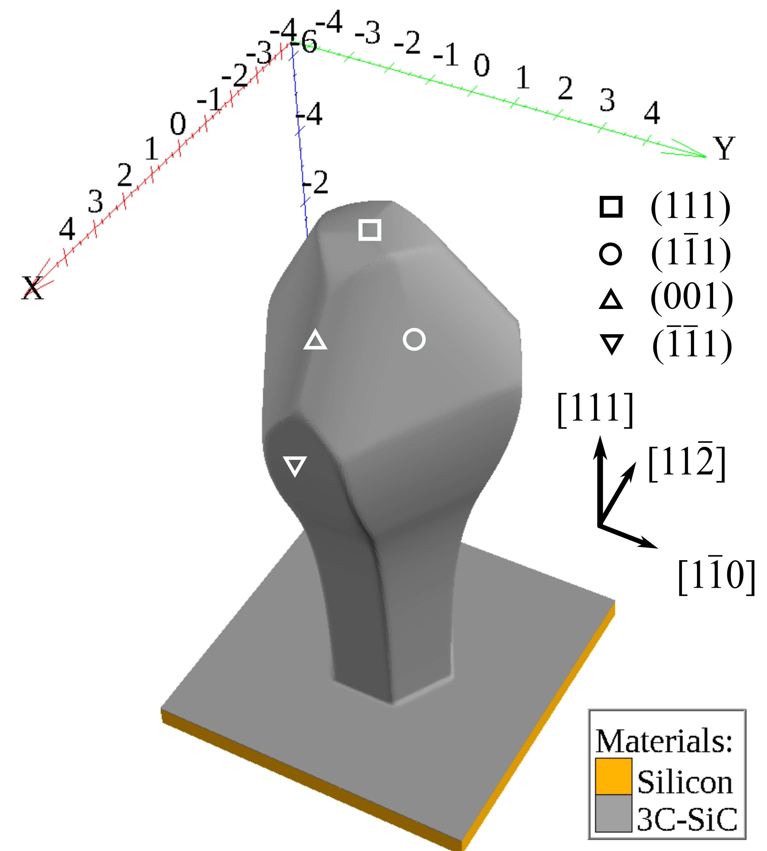
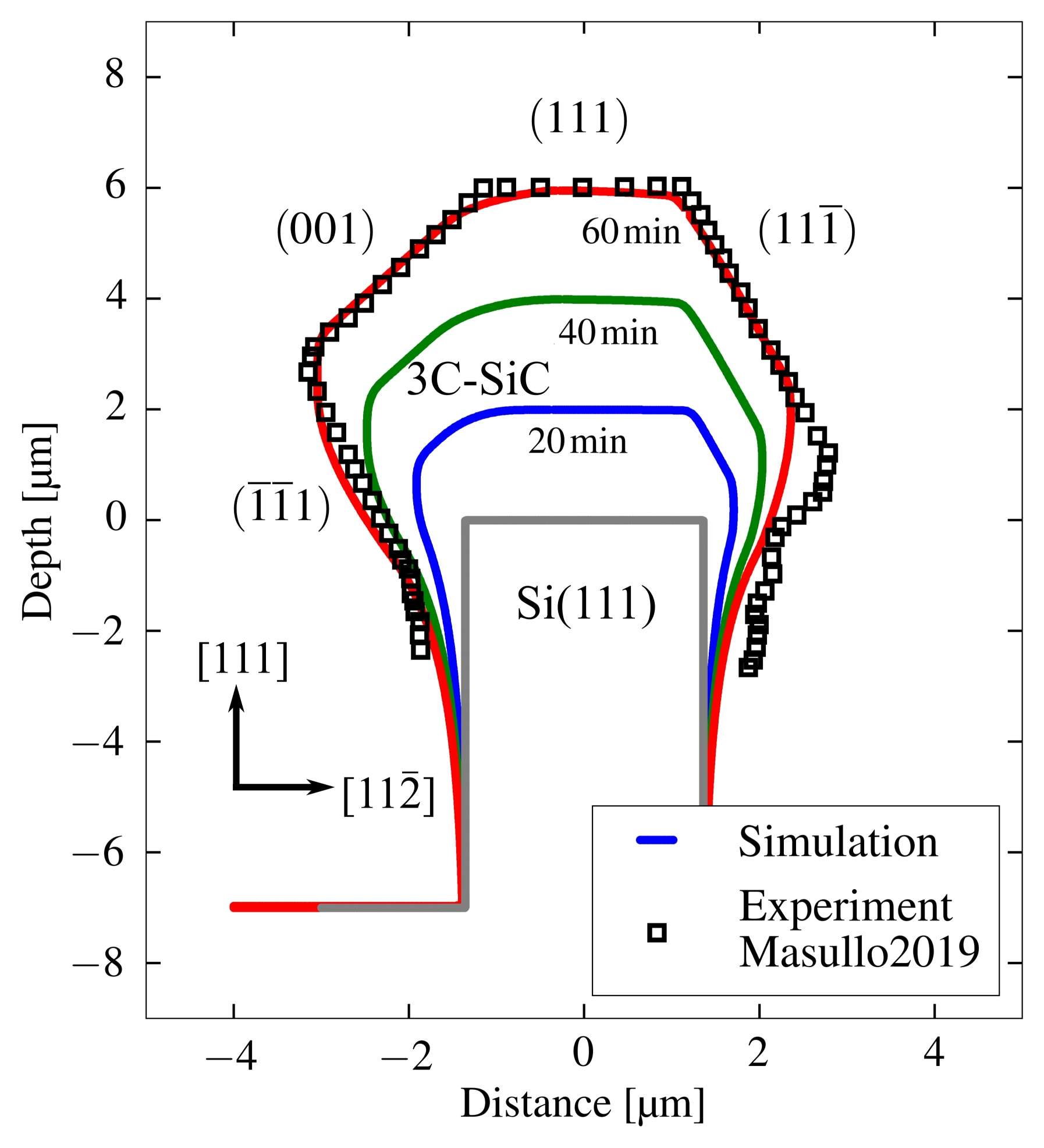
The exponentially decreasing flux modulates the crystal growth rates for different topography heights, which results in a model with six parameters, as summarized in Tab. 5.2. The parameters are calibrated based on the experimental SEM images presented in Ref. [83]. The calibrated model is employed in the CA engine (4.36) using  , where a stable 3D simulation of the growth process is achieved. The resulting geometry is depicted in Fig. 5.11a and shows a characteristic shape. In the upper
regions the crystal facets
, where a stable 3D simulation of the growth process is achieved. The resulting geometry is depicted in Fig. 5.11a and shows a characteristic shape. In the upper
regions the crystal facets  ,
,  ,
,  , and
, and  are formed. In the lower regions the exponentially decreasing diffusive flux results in a decreasing film thickness. The experimentally observed shape and the simulated profile are compared in Fig. 5.11b, where a cross-section is shown for 60 min growth time.
Additionally, the predicted topographies for 20 min and 40 min are shown. As can be seen from the 60 min comparison, the main crystal facets are well reproduced. However, there is some deviation in the
lower parts of the  facet. In the simulation this facet is smaller in extension, because the diffusive region of the exponentially decreasing 3C-SiC film thickness is determined by the widest point, which is defined by edge formed by and . The simulation domain below the vertical coordinate of this edge is globally considered as diffusive region. Improvements of these deviations are expected if a more sophisticated flux calculation, e.g., top-down ray-tracing
is employed.
facet. In the simulation this facet is smaller in extension, because the diffusive region of the exponentially decreasing 3C-SiC film thickness is determined by the widest point, which is defined by edge formed by and . The simulation domain below the vertical coordinate of this edge is globally considered as diffusive region. Improvements of these deviations are expected if a more sophisticated flux calculation, e.g., top-down ray-tracing
is employed.
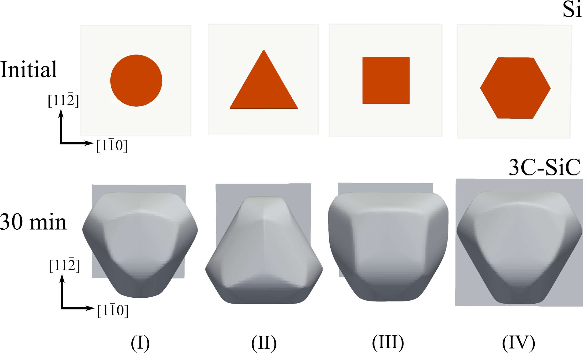
Once the growth model is calibrated, several initial Si pillar geometries can be investigated. Section 5.12 presents the resulting facets for cyclic, triangular, and
square base area after 30 min growth time. On the one hand, these results show the complexity of possible topographies. On the other hand, a relatively high resolution ( ) is required to achieve high quality shapes in regions where multiple facets coincide. In particular in three dimensions, it is possible that three or more facets coincide and thus form complex structures. Inherent rounding
of corners is always present in the level-set method, even though in this case the developed CA engine minimizes additional numerical dissipation (cf. Fig. 4.9). Thus, in regions of high geometric complexity, a high grid resolution is needed. At the same time there are also effectively flat
regions, where a significantly smaller number of grid points is sufficient to resolve the topography. A possible improvement is discretization with adaptive resolution, where regions of high curvature are highly-resolved. Nevertheless,
the 3C-SiC heteroepitaxy applications demonstrate that the devised crystal symmetry-respecting interpolation scheme is well-suited to construct a growth rate model which allows for good agreement with experimental observations.
The heteroepitaxy application presented in this section demonstrates that complex 3D topographies can emerge during an anisotropic process and are properly described by developed CA engine. An application that specifically takes advantage of complex 3D topographies is the anisotropic wet etching of sapphire, which is employed to improve LEDs and is presented in the following section.
5.4 Anisotropic Wet Etching of Patterned Sapphire Substrates
Anisotropic wet etching of sapphire substrate is a fabrication process which results in particularly complex topographies. Sapphire substrates are commonly employed in the field of LEDs. In order to fabricate GaN-based blue-light LEDs, high-quality GaN films are essential. Ground breaking advancements in metalorganic vapor phase epitaxy and buffer technology initiated the breakthrough of blue-light LEDs [159]. These advancements subsequently enabled high-quality GaN films grown on sapphire substrates and emerged to a mature technology for a variety of applications in recent years [160]. One example is the silicon-on-sapphire technology platform, which enables integrated waveguides [161] and sensor applications [162]. The topography of sapphire substrates plays an important role for performance of GaN-based LEDs. A patterned sapphire substrate (PSS) provides multiple advantages. In terms of crystal quality, techniques like lateral epitaxial overgrowth reduce the number of threading dislocations and defect in GaN films. The performance of the ultimate LED is also enhanced by improving the light extraction efficiency (LEE) with non-planar sapphire-GaN interfaces [163]. This topographical aspect is important for the design of GaN-based LEDs and is discussed in depth in Section 6.2.
PSSs are fabricated in a multi-step process which is illustrated in Fig. 5.13. The initially planar substrates are typically first etched with inductively coupled
plasma RIE. A subsequent photoresist reflow process during hard-bake [160], [164], [165] allows for the patterning of different geometries: Cones, cylinders,
hemispheres [166], and pyramids [167] have been presented. In all cases,
periodic patterns with specific net surface coverage (measuring the fraction of the wafer filled with patterns) are produced. Surface coverage typically does not exceed the threshold of around 70%, because nucleation sites on flat
parts of the wafer need to be present to enable high-quality epitaxy [160]. The patterned arrays can be further processed using anisotropic wet etching
techniques [168]. The most commonly utilized anisotropic wet etchants for single-crystal sapphire are mixtures of  and
and  [105], [106], [169]–[171]. Alternatively, recent research also investigates KOH [172]. The resulting etch profiles exhibit complex topographies, due to the trigonal symmetry of sapphire. Moreover, the observed characteristic crystal facets have
high Miller-Bravais indices suggesting an intricate etch anisotropy. Due to the strong impact on the LEE of the final LED, precise control over the resulting 3D topography is essential. Thus, geometry-focused modeling and
simulation approaches facilitate the optimization of the wet etching step with respect to etch time, temperature, and etchant mixture. In particular, a continuum level-set based description of the wet etching process is well-suited to
satisfy the needs of engineering-focused process TCAD workflows [25], [121], [122].
[105], [106], [169]–[171]. Alternatively, recent research also investigates KOH [172]. The resulting etch profiles exhibit complex topographies, due to the trigonal symmetry of sapphire. Moreover, the observed characteristic crystal facets have
high Miller-Bravais indices suggesting an intricate etch anisotropy. Due to the strong impact on the LEE of the final LED, precise control over the resulting 3D topography is essential. Thus, geometry-focused modeling and
simulation approaches facilitate the optimization of the wet etching step with respect to etch time, temperature, and etchant mixture. In particular, a continuum level-set based description of the wet etching process is well-suited to
satisfy the needs of engineering-focused process TCAD workflows [25], [121], [122].

The etch profile evolution with the emerging crystal facets has been experimentally characterized by many research groups [105], [171], [173]–[176]. However, the
etch rate anisotropy of single-crystal sapphire is still being investigated. Most importantly, etch rate anisotropy of sapphire has been confirmed to be significantly more intricate than typically observed with . Only a small number of etch rate/crystal direction pairs have been identified and the reported pairs are not consistent throughout these studies. Recent efforts to comprehensively characterize various etching solutions
and temperatures [106] have provided additional insights into the etching anisotropy of sapphire.
In general, there are two options to approach level-set models for anisotropic wet etching of sapphire. One option is to perform elaborate experimental characterization and incorporate a large number of etch rates into the model calibration process. Zhang et al. [120] have employed hemisphere etching experiments to reveal a large number of crystal directions and etch rates in order to construct a level-set model. The second option is based on standard (sparse) characterization data from a limited set of SEM images and AFM measurements. Given a small set of identified characteristic crystal facets a specialized interpolation technique is required to reflect the intricate anisotropy of sapphire.
In the following, the second option is discussed. After the construction of the etch rate distribution is presented, the model calibrated is discussed. Finally, the simulation results are compared with experimental results.
5.4.1 Etch Rates in Trigonal Symmetry

 . Crystal directions are indicated with
  ,
,  ,
,  ,
,  ,
,  ,
,  , and
, and  (following the nomenclature of Ref. [174]) and constitute characteristic directions related to wet etching
of sapphire. The general direction ’
(following the nomenclature of Ref. [174]) and constitute characteristic directions related to wet etching
of sapphire. The general direction ’  ’ is reduced to the crystallographically equivalent direction ’
  ’ by employing a series of symmetry operations. (b) Flowchart of the algorithm to reduce a general direction (input) to the equivalent direction residing in the fundamental domain (output). The z-component of the Cartesian representation of is denoted with
  and
and  indicates the polar angle of in spherical coordinates.
Reprinted with adaptions from Toifl et al., Semicond. Sci. and Technol. 36 (4), p. 045016. [122] (2021). © 2021 Authors, licensed under the Creative Commons Attribution 4.0 License (http://creativecommons.org/licenses/by/4.0/).
As discussed in Section 3.1, the foundation of the modeling approach is the kinetically limited nature of anisotropic wet etching of sapphire.
This has also been confirmed by experimental studies [174]–[176]. Thus, an etch rate
distribution can be defined and employed for computing the etch profile evolution. Sapphire exhibits ditrigonal scalenohedral symmetry in the trigonal system (point group in Schönflies notation) [177], [178] with the associated symmetry operations depicted in Fig. 5.8. In order to reflect symmetry, the procedure outlined in Section 5.3.1 is followed. The fundamental domain is the spherical triangle illustrated in Fig. 5.14a [41]. The algorithm for reducing a general direction to is given in Fig. 5.14b. The crystal symmetry operations which are used are point inversion,  -rotation about the
  -axis, and reflection at the
  -plane which is spanned by
 ![\( \left [\overline {1}\, 1\, 0\, 0\right ] \)](PhD_Thesis-images/D85E0B0F98A4236DDAAFFCA7D37260BA.svg) and
and ![\( \left [ 0\, 0\, 0\, 1\right ] \)](PhD_Thesis-images/3AA69B3ECAA94522D1320892646A3C0D.svg) . After the reduction procedure all directions on the unit sphere are mapped into . Thus, it is sufficient to perform interpolation only on this subset of the sphere.
. After the reduction procedure all directions on the unit sphere are mapped into . Thus, it is sufficient to perform interpolation only on this subset of the sphere.
While trilinear or spherical barycentric coordinates-based interpolation techniques have been successfully employed in the previous sections, these approaches demand a large set of known etch rates to account for the intricate etch anisotropy of sapphire. In particular, multiple local minima and maxima are prevalent [106], as illustrated in Fig. 5.15. The structure of the experimentally observed anisotropy motivates an interpolation approach based on the parametrization

 denotes an isotropic distribution, extended by a sum of power cosine distributions. These are centered around a given crystal direction
  .
.  refers to the Heaviside function and indicates the scalar product. With this parametrization, spatially confined extrema are determined by the coefficients
  . The weighting factors
  define the width of maxima and minima. A similar parametrization has been proposed by Siem and Carter [179] and has also more recently been employed in phase-field growth simulations [88], [180]. The coefficients can be associated with the etch rates
  by demanding
  , which results in a linear system of equations. With (5.10) the extrema can be resolved even for a small number of known etch rate/crystal direction
pairs. No triangulation is required, and thus it is not necessary to include supplemental rates at the boundary of the fundamental domain. This ensures that the fundamental domain is fully covered with triangles.
, which results in a linear system of equations. With (5.10) the extrema can be resolved even for a small number of known etch rate/crystal direction
pairs. No triangulation is required, and thus it is not necessary to include supplemental rates at the boundary of the fundamental domain. This ensures that the fundamental domain is fully covered with triangles.
To summarize, the parametrization (5.10) provides the capability to construct the etch rate distribution if only a limited number of characterized crystal facets is available. Hence, the engineering-focused modeling of sapphire wet etching is enabled, which is discussed in the following section.

 at
at  . Crystal directions corresponding to the characteristic facets , , etc. are shown.
Reprinted with permission from Toifl et al., Semicond. Sci. and Technol. 36 (4), p. 045016. [122] (2021). © 2021 Authors, licensed under the Creative Commons Attribution 4.0 License (http://creativecommons.org/licenses/by/4.0/).
5.4.2 Modeling and Results
In the following, the experimental setup to anisotropically etch sapphire, as presented in a comprehensive study by Shen et al. [174]–[176], is considered. The experiments act as reference for the presented level-set modeling approach and will be used to evaluate the approach. First, the c-plane sapphire
substrate was patterned to fabricate an array of cones with hexagonal symmetry (3.2 µm pitch). The cones have a base diameter of 2.93 µm. Second, the array was etched with several mixtures
of and at various temperatures. The etchant solutions are referred to as MX-Y, where X-Y indicates a volume ratio of  . The characterization of the topography was performed with SEM and AFM. Furthermore, the crystal facets appearing during etching were identified by determining the Miller-Bravais indices. The topographical change
was documented for several etch times. Fig. 5.16 illustrates the topography evolution for one of these experiments (originally published in [175]).
. The characterization of the topography was performed with SEM and AFM. Furthermore, the crystal facets appearing during etching were identified by determining the Miller-Bravais indices. The topographical change
was documented for several etch times. Fig. 5.16 illustrates the topography evolution for one of these experiments (originally published in [175]).
at .Reprinted from Shen et al., ECS J. Solid State Sci. Technol. 6 (9) (2017), R122-R130 [175]. © 2017 Authors, licensed under the Creative Commons Attribution 4.0 License (http://creativecommons.org/licenses/by/4.0/).
Basic Structure of the Etch Rate Distribution
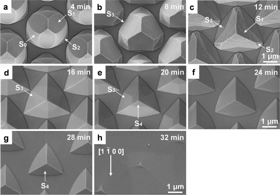
Since the parametrization (5.10) incorporates directions associated with minimal and maximal etch rates, the experimental observations can be utilized to
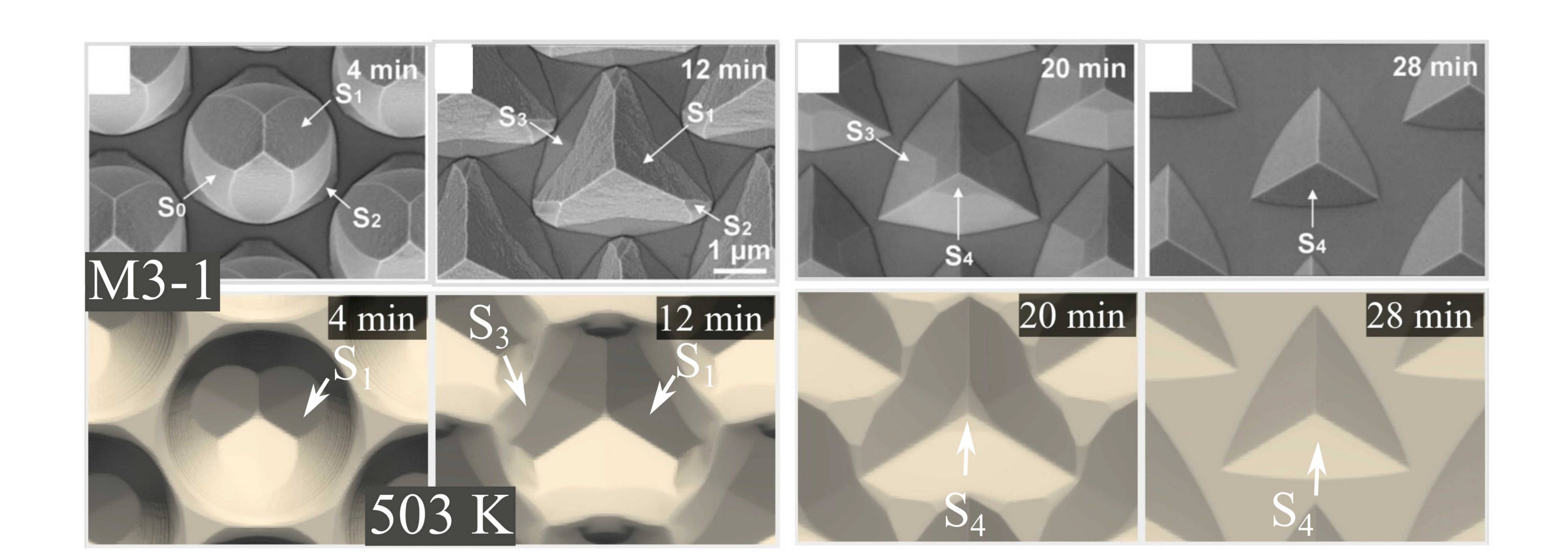
deduce the structure of the etch rate distribution . As shown in Fig. 5.16, in a typical etch process starting with initial conical shape a crystal facet 3 with very high etch rates first emerges near the apex (a). A slower etching facet can be observed after 8 min at the base. As etching proceeds, replaces (d). Furthermore, the facet is emerging at the top of the structure and is eventually dominating (f) before the entire initial topography is entirely etched away. All experiments presented by Shen et al. show a similar sequence of
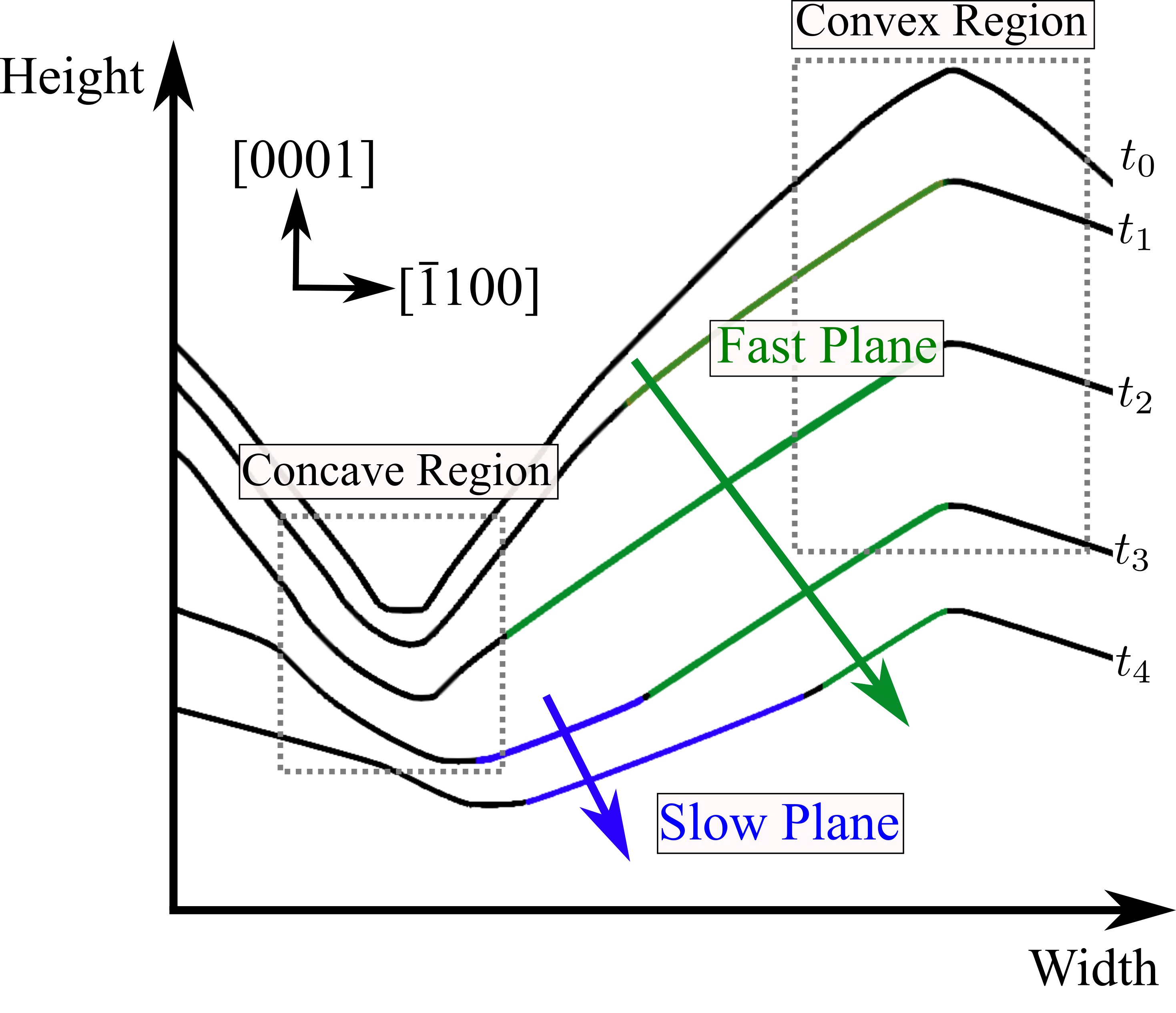
facets appearing at apex and base, until the c-plane wafer surface becomes predominant again. For the subsequent discussions, the local convexity of the topography is significant. Fig. 5.17 illustrates the cross-section of the experiment for different etch times. The cone’s apex is locally a convex region, whereas the base forms a concave region. As pointed
out in Section 3.2.2, rapidly etching facets (fast planes) dominate the topography evolution in convex regions, while slowly etching
facets (slow planes) define the geometry in concave regions. Hence, facets appearing in a convex region are etched faster than all neighboring facets with similar Miller indices. Thus, has necessarily a local maximum at the corresponding direction. Similarly, facets appearing in concave region require to have local minima at the corresponding directions . In the present experiment, the etch rates of facets and constitute local maxima, while facet is a local minimum (see Fig. 5.15). The calibration process of the etching model is facilitated by incorporation of this structural information.
Reprinted with permission from Toifl et al., Semicond. Sci. and Technol. 36 (4), p. 045016. [122] (2021). © 2021 Authors, licensed under the Creative Commons Attribution 4.0 License (http://creativecommons.org/licenses/by/4.0/).
3 In order to facilitate the discussion in this thesis, the original nomenclature of Ref. [174] is used. Hence, topographical regions of
interest and crystal facets are identified as  .
.
Model Calibration
The practical construction of is based on the experimental characterization of the crystal facets provided by Shen et al. [174]–[176]. Thus, the measured Miller-Bravais indices  are converted to the Cartesian representation of the facet normal vector [156]

where the lattice constant ratio for sapphire  is assumed as 12.991 Å / 4.785 Å.
  ,
,  , and
, and  reside within the c-plane and
  is perpendicular to the c-plane. These directions constitute the basic framework for . In order to fine-tune , the model parameters in (5.10) are calibrated with respect to AFM data and SEM images. Tab. 5.3 shows all combinations of process temperatures and etchant mixtures (referred to as etching experiments in the following) investigated in Ref. [174]. SEM images are available for eleven etching experiments and one set of AFM profiles consisting of multiple etch times
for M3-1 at
is perpendicular to the c-plane. These directions constitute the basic framework for . In order to fine-tune , the model parameters in (5.10) are calibrated with respect to AFM data and SEM images. Tab. 5.3 shows all combinations of process temperatures and etchant mixtures (referred to as etching experiments in the following) investigated in Ref. [174]. SEM images are available for eleven etching experiments and one set of AFM profiles consisting of multiple etch times
for M3-1 at  . These experimental results are the reference for the subsequently discussed level-set set simulations and analyses conducted via Silvaco Victory Process [140], where the developed CA engine (4.36) is employed with
  . Since the focus is on the wet etching step, the pre-patterning of the cones is emulated to perfectly match the initial AFM profile (prior to the anisotropic wet etching step).
The model calibration target is to achieve the best possible visual congruence between simulated topography and SEM images for all available etch times. Furthermore, the orientation of the local surface normals of the level-set topography are inspected, confirming the emergence of correct crystal facets. Since the SEM images show the topography from a top view, the etch rate of the c-plane substrate cannot be unambiguously determined. Thus, the experimentally measured c-plane etch rates presented in Ref. [175] are employed as a reference to ensure a correct etch rate of the c-plane etches in the simulation.
indicates SEM images and the symbol  denotes AFM profiles which characterize multiple etch times.
Reprinted with permission from Toifl et al., Semicond. Sci. and Technol. 36 (4), p. 045016. [122] (2021). © 2021 Authors, licensed under the Creative Commons Attribution 4.0 License (http://creativecommons.org/licenses/by/4.0/).
Temperature ![\( \left [\si {\kelvin }\right ] \)](PhD_Thesis-images/4F30E05D1CC759F226A11E122BA480CC.svg) |
||||
| Etchant | 473 | 503 | 523 | 543 |
| M5-1 | |
|
|
|
| M3-1 |  |
|||
| M1-1 | |
|||
| M1-3 | |
|||
| M0-1 | |
|
|
|
First, the etching experiment with M3-1 at is considered. In the experiments, Shen et al. have characterized three crystal facets:  ,
,  ,
,  . Thus, needs to have a local minimum along and local maxima along and . The experimental topography evolution (Fig. 5.16) shows the immediate formation of , which implies that the etch rate of
  (
(  ) is greater than or equal to the etch rate of
  (
(  ). Otherwise, would emerge near the top of the cone. With these boundary conditions, the model parameters are fine-tuned based on the congruence of SEM image and simulation results. Tab. 5.4 shows the resulting parameters for the calibrated model. The best congruence for the entire etch profile evolution is achieved by broadening the maximum along . The broadening is essential for the formation of the subsequently appearing facet . In an experimental study by Xing et al. [106] broadened maxima have been reported
for etchants M1-1 and M3-1 as well albeit at the slightly different etching temperature of 509 K. This confirms that broadening is an essential property which needs to be incorporated into the modeling to
properly predict the final topography. The broadening is implemented by incorporating only one additional direction which corresponds to a
). Otherwise, would emerge near the top of the cone. With these boundary conditions, the model parameters are fine-tuned based on the congruence of SEM image and simulation results. Tab. 5.4 shows the resulting parameters for the calibrated model. The best congruence for the entire etch profile evolution is achieved by broadening the maximum along . The broadening is essential for the formation of the subsequently appearing facet . In an experimental study by Xing et al. [106] broadened maxima have been reported
for etchants M1-1 and M3-1 as well albeit at the slightly different etching temperature of 509 K. This confirms that broadening is an essential property which needs to be incorporated into the modeling to
properly predict the final topography. The broadening is implemented by incorporating only one additional direction which corresponds to a  facet. The associated etch rate is set as
  , which keeps the number of model parameters at a minimum while still allowing for - as will be shown - accurate simulation results.
).Reprinted with permission from Toifl et al., Semicond. Sci. and Technol. 36 (4), p. 045016. [122] (2021). © 2021 Authors, licensed under the Creative Commons Attribution 4.0 License (http://creativecommons.org/licenses/by/4.0/).
| M3-1 |  |
Directions | |||||
| C | , |
|
|
|
|
||
Weights  |
200 | 100 | 60 | 100 | 100 | ||
Etch Rates  [ [  ] ] |
24 | 59 | 36 | 57 | 39 | 8 | |
| M1-1 | |
Directions | |||||
| C | , |
|
|
|
|
||
| Weights |
200 | 100 | 60 | 100 | 100 | ||
| Etch Rates [ ] |
18 | 60 | 37 | 52 | 36 | 7 | |
| M1-3 | |
Directions | |||||
| C | , |
|
|
|
|
||
| Weights |
200 | 100 | 60 | 100 | 100 | ||
| Etch Rates [ ] |
16 | 62 | 39 | 51.5 | 34 | 8 | |
Reprinted with permission from Toifl et al., Semicond. Sci. and Technol. 36 (4), p. 045016. [122] (2021). © 2021 Authors, licensed under the Creative Commons Attribution 4.0 License (http://creativecommons.org/licenses/by/4.0/).
. On the left half of the illustrated cone profile the crystal facets , , and are observed, while the right half outlines ridges of the topography where two crystallographically equivalent topography zones coincide.Reprinted with permission from Toifl et al., Semicond. Sci. and Technol. 36 (4), p. 045016. [122] (2021). © 2021 Authors, licensed under the Creative Commons Attribution 4.0 License (http://creativecommons.org/licenses/by/4.0/).
Therewith, the broadened maximum is effectively created by the superposition of two terms in the parametrization (5.10), corresponding to and . Furthermore, a direction corresponding to  is included, which is a facet characterized by Shen et al. for M5-1 experiments and ensures that the
 ![\( \left [ 0\,0\,0\,1\right ] \)](PhD_Thesis-images/C22720C2F64CAB39B9A5F2B2C2CE4DDA.svg) (c-direction) constitutes a local minimum. The inclusion of
(c-direction) constitutes a local minimum. The inclusion of  is also consistent with the characterization presented in [106].
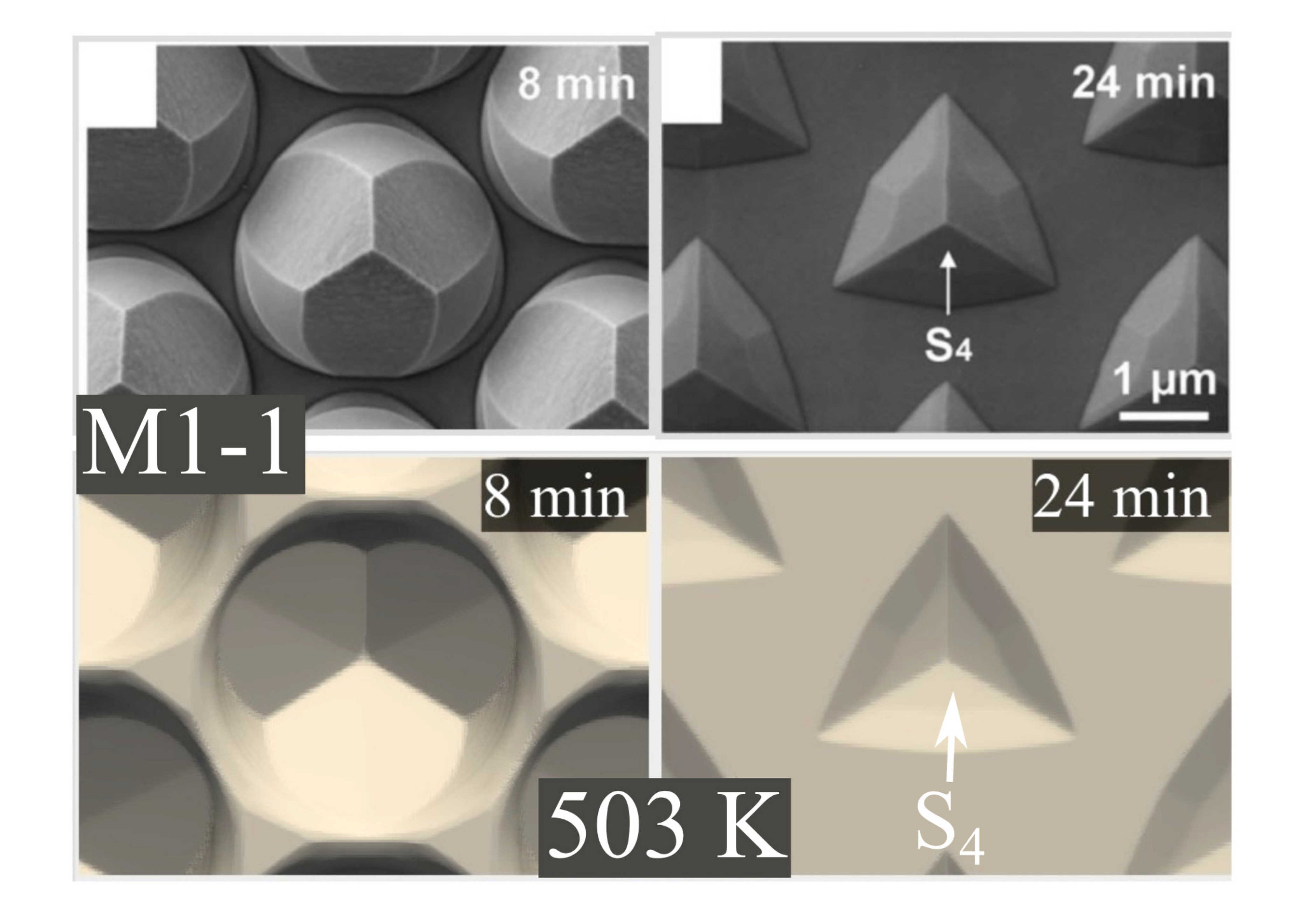
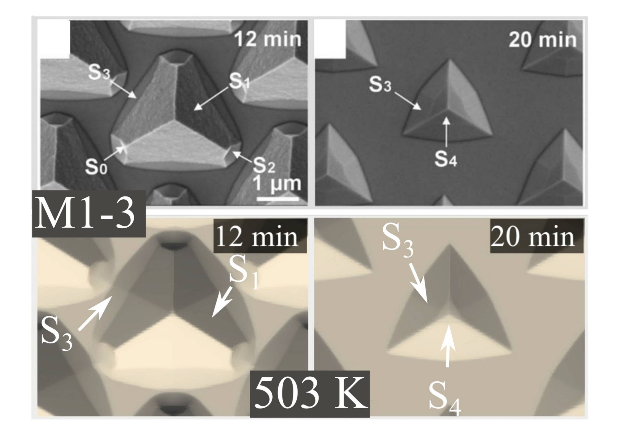
The simulation results for etchant mixture M3-1 are compared with SEM images in Fig. 5.18a. Solid congruence over the entire range of available etch times
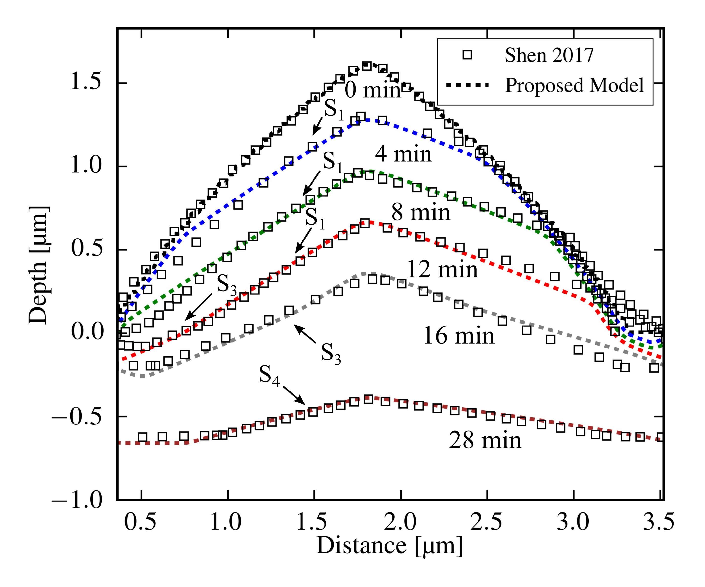
(4 min to 28 min) is demonstrated. The developed modeling approach is validated by considering the 2D etch profiles of the PSS along in Fig. 5.19. The simulated profiles closely match the experimental AFM results, which indicates that the optimization of visual congruence and incorporating the
experimental values for  indeed results in suitable expressions for . Thus, the calibration procedure can be repeated to construct for etchant mixtures M1-1 and M1-3 at . Tab. 5.4, Fig. 5.18b, and Fig. 5.18c present the parameters and simulation results, respectively. Importantly, the resulting models for M3-1, M1-1, and M1-3 have the same set of directions and the exact
same values for the weights
indeed results in suitable expressions for . Thus, the calibration procedure can be repeated to construct for etchant mixtures M1-1 and M1-3 at . Tab. 5.4, Fig. 5.18b, and Fig. 5.18c present the parameters and simulation results, respectively. Importantly, the resulting models for M3-1, M1-1, and M1-3 have the same set of directions and the exact
same values for the weights  .
.
Temperature Dependence
Furthermore, Shen et al. have presented SEM images at several temperatures (473 K, 503 K, 523 K, and 543 K) for etchants M0-1 and M5-1. In the associated experiments a
structural difference between the solution (M0-1) and the mixture M5-1 has been observed [176]. The former results in the
formation of a facet  instead of . The latter exhibits a similar topography evolution as discussed before. facets have not been observed for any of the investigated temperatures in case of M0-1. Again, the topography evolution argument can be applied to deduce that the corresponding
  constitutes a local minimum of , even though is only slightly smaller than the local maximum . Consequently, is etched away before evolves from the top of the structure. Further fine-tuning results in high accuracy models, as shown in Fig. 5.20a and Fig. 5.20b. The model parameters are presented in Tab. 5.5.
has been calibrated for four different temperatures. Thus, the temperature dependence of the model etch rates and the isotropic component can be investigated. Fig. 5.21 depicts the etch rate distributions and the etch rates in a semi-logarithmic Arrhenius plot. Accurate results are achieved by
using the same set of weights for all temperatures, which indicates a fundamental temperature-independent general form of . The etch rates distributions in Fig. 5.21a and Fig. 5.21c are shown along the paths that
are illustrated in the insets. While path exclusively follows the boundaries of the fundamental domain, path  includes the direction which is located offside the boundary
  . Furthermore, the M5-1 model is characterized by the same
  as the M3-1, M1-1, and M1-3 models. The resulting etch rates of M0-1 and M5-1 exhibit a temperature dependence which is well-described by an Arrhenius law

where is the etch rate (also including the isotropic component ),  refers to a pre-exponential coefficient,
  denotes the activation energy in eV,
  is the Boltzmann constant, and
  refers to the etching temperature. The Arrhenius plots in Fig. 5.21b and Fig. 5.21d, respectively,
show that all
refers to the etching temperature. The Arrhenius plots in Fig. 5.21b and Fig. 5.21d, respectively,
show that all  and follow an Arrhenius law. By employing standard Arrhenius fitting, the pre-exponential coefficients and activation energies are determined and the resulting values are presented in Tab. 5.5.
). The etch rates follow an Arrhenius law (5.12) with parameters and .Reprinted with permission from Toifl et al., Semicond. Sci. and Technol. 36 (4), p. 045016. [122] (2021). © 2021 Authors, licensed under the Creative Commons Attribution 4.0 License (http://creativecommons.org/licenses/by/4.0/).
| M0-1 | Directions | |||||
| C | |
|
|
|
|
|
| Weights |
200 | 100 | 100 | 100 | 100 | |
| A [ ] |
5.296 × 10¹⁰ | 4.897 × 10¹⁰ | 6.953 × 10¹⁰ | 1.407 × 10¹⁰ | 8.894 × 10¹⁰ | 3.236 × 10¹¹ |
| [eV] |
0.962 | 0.882 | 0.909 | 0.862 | 0.923 | 1.054 |
| M5-1 | Directions | |||||
| C | |
|
|
|
|
|
| Weights |
200 | 100 | 60 | 100 | 100 | |
| A [ ] |
1.667 × 10¹¹ | 7.551 × 10¹¹ | 5.378 × 10¹¹ | 6.444 × 10¹¹ | 9.042 × 10¹¹ | 5.444 × 10¹² |
| [eV] |
0.974 | 1.018 | 1.021 | 1.011 | 1.039 | 1.152 |
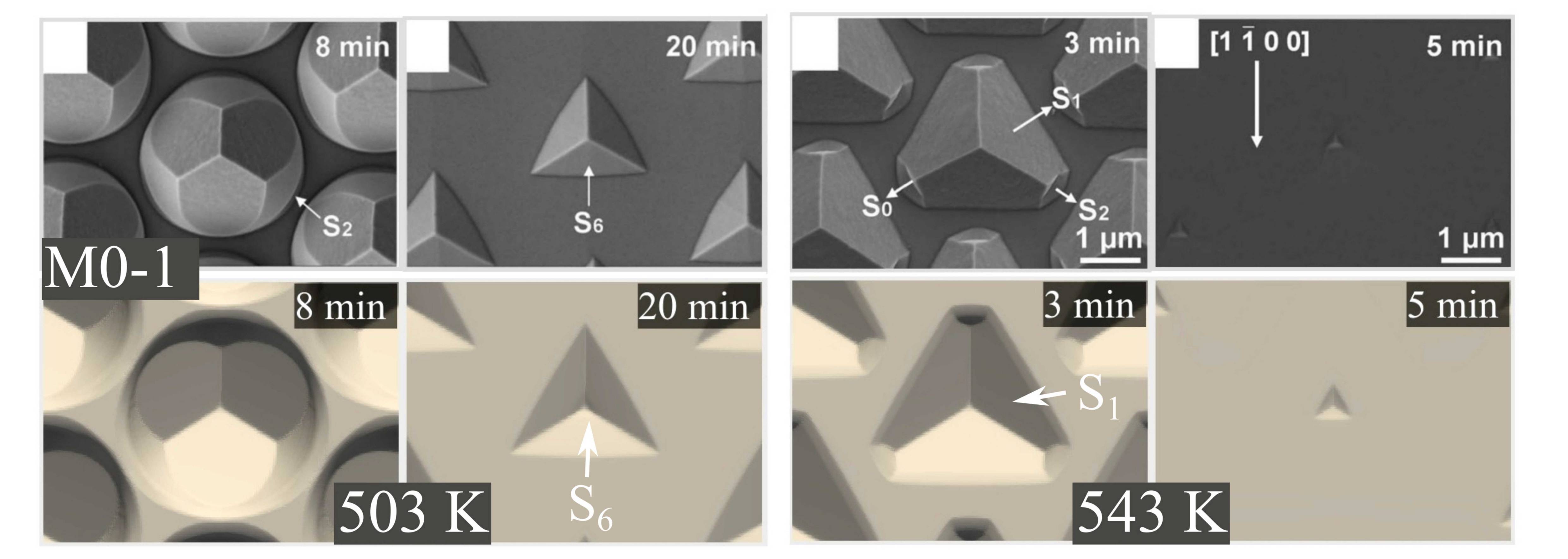
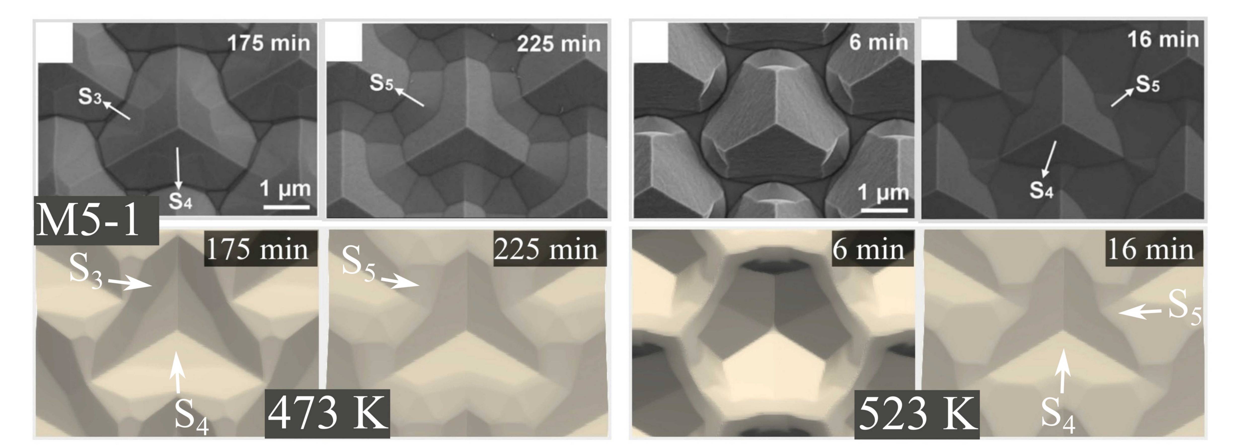
Reprinted with permission from Toifl et al., Semicond. Sci. and Technol. 36 (4), p. 045016. [122] (2021). © 2021 Authors, licensed under the Creative Commons Attribution 4.0 License (http://creativecommons.org/licenses/by/4.0/).


Reprinted with permission from Toifl et al., Semicond. Sci. and Technol. 36 (4), p. 045016. [122] (2021). © 2021 Authors, licensed under the Creative Commons Attribution 4.0 License (http://creativecommons.org/licenses/by/4.0/).
Discussion of the Anisotropic Wet Etching Model
The etch rates of mixtures M0-1 and M5-1 display high activation energies  in the temperature range from 473 K to 543 K, which is consistent with the assumption of reaction-limited etching. Thus the modeling approach with a crystal orientation-dependent etch rate
distribution is justified. As shown in Fig. 5.21, for constant temperatures the etch rate values associated with the defining crystal directions are all in the same order of
magnitude. Nevertheless, the etch rate distribution is complex, due to the multiple local extrema. Moreover, the defining crystal directions all reside in a section that is smaller than a quarter of the fundamental domain (see
Fig. 5.14a). Consequently, the evolving crystal facets have similar Miller-Bravais indices, thus leading to the intricate etch anisotropy of sapphire. The rates
obtained when modeling the temperature dependence by an Arrhenius law enable high-quality etching models for etchants M0-1 and M5-1 in the temperature range from 473 K to 543 K.
in the temperature range from 473 K to 543 K, which is consistent with the assumption of reaction-limited etching. Thus the modeling approach with a crystal orientation-dependent etch rate
distribution is justified. As shown in Fig. 5.21, for constant temperatures the etch rate values associated with the defining crystal directions are all in the same order of
magnitude. Nevertheless, the etch rate distribution is complex, due to the multiple local extrema. Moreover, the defining crystal directions all reside in a section that is smaller than a quarter of the fundamental domain (see
Fig. 5.14a). Consequently, the evolving crystal facets have similar Miller-Bravais indices, thus leading to the intricate etch anisotropy of sapphire. The rates
obtained when modeling the temperature dependence by an Arrhenius law enable high-quality etching models for etchants M0-1 and M5-1 in the temperature range from 473 K to 543 K.
Furthermore, the activation energies of the defining crystal rates differ less than 10% (with the exception of the isotropic component ). The small difference does not result in a different order of appearance and disappearance of crystal facets at different temperatures. Accordingly, there are no intersections of the Arrhenius line in the temperature range
from 473 K to 543 K.
In summary, a continuum model for wet etching of sapphire with mixtures of and has been proposed and verified. The model enables the simulation and analysis of the emerging 3D topographies during an anisotropic wet etching step with different time and temperature.
5.5 Summary
In this chapter, continuum level-set simulations for four representative anisotropic process steps were presented. All considered process steps are essential to fabricate state-of-the-art semiconductor devices and include anisotropic wet etching, heteroepitaxy, and selective epitaxy. Continuum etch and growth rate models were proposed to describe the 2D and 3D topography evolution. In order to account for the distinctive crystal facets emerging from heteroepitaxy of 3C-SiC and wet etching of sapphire, interpolation procedures, reflecting the associated tetrahedral and trigonal crystal symmetry, were proposed. The interpolation procedures are based on the idea of mapping arbitrary crystal directions to the fundamental domain of the crystal symmetry class.
The particularly intricate wet etching anisotropy of sapphire was captured with a flexible parametrization that enables the construction of high-quality etch rate distributions, even if only a small set of experimentally characterized crystal facets is available. The continuum models were employed in conjunction with the developed CA engine (Chapter 4), which now enables numerically reliable and accurate topography simulations. The simulation results were compared with experimental observations (AFM, SEM, TEM) from the literature, confirming that the presented models capture the experimentally obtained topography features with high accuracy. Hence, the capability of the presented topography-focused continuum modeling approach was clearly demonstrated.
In the following chapter, semiconductor process simulation is discussed in the broader perspective of TCAD. In particular, the model for anisotropic wet etching of sapphire is employed to determine the wet etching process parameters needed to optimize GaN-based LEDs with sapphire substrates.