In our group a new physics-based modeling approach was developed and verified. This approach is based on TCAD device simulators, thereby providing good degradation results on the device level which can be used for reliable device lifetime prediction. The model spans from the microscopic level of interface defect generation up to the device level. The microscopic level considers SP and MP processes relying on the carrier energy distribution functions for electrons and holes. As for the device level, the drift-diffusion device simulation technique allows to extract the device parameter degradation. This gives the unique possibility to define the life-time using the design relevant attributes instead of simply dealing with trap concentrations. This is especially important, since the trap creation is highly localized and the effective device degradation depends on the position of the traps in the channel. The full device simulation step used in this approach gives a more accurate physical link between generated traps and device parameter degradation.
Like in the models by Hess and Bravaix, it is distinguished between
single-particle and a multiple-particle components. In the first realizations
of this model, only electrons were considered, giving good results for
n-channel MOS devices with a channel length of 0.5 µm
[17,245]. Later, also secondary generated holes were considered and consolidated by the
model [18], as already proposed by other authors,
e.g. Moens et al. [246,247]. The degradation mechanism is driven by
the acceleration integrals (
![]() and
and
![]() ) which are similarly defined as
in the approaches by Hess and Bravaix, compare (6.4). These
carrier acceleration integrals for the SP and MP process are
) which are similarly defined as
in the approaches by Hess and Bravaix, compare (6.4). These
carrier acceleration integrals for the SP and MP process are
| (6.27) |
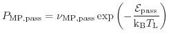
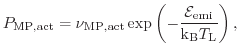
The interface state generation rate for the SP process in this model is assumed
to be described by a first-order chemical reaction with the activation rate
![]() giving
giving
Like in the Bravaix approach, a truncated harmonic oscillator is employed to describe the bond energetics. However, we write the rate equations for the last bonded state in a different fashion: defined as
 |
(6.35) |
 |
(6.36) |
using the energy barriers as shown in Fig. 6.2 and the
attempt frequencies
![]() and
and
![]() The
passivation reaction depends on the existence of a dangling bond and the
existence of a hydrogen atom which can passivated, making this a second-order
reaction. The density of dangling bonds is equal to the density of generated
traps. No initial free hydrogen is assumed, so the available number of hydrogen
atoms corresponds to the number of generated traps. This leads to the quadratic
dependence
The
passivation reaction depends on the existence of a dangling bond and the
existence of a hydrogen atom which can passivated, making this a second-order
reaction. The density of dangling bonds is equal to the density of generated
traps. No initial free hydrogen is assumed, so the available number of hydrogen
atoms corresponds to the number of generated traps. This leads to the quadratic
dependence
![]() in (6.34). To satisfy the
dimensionality, the passivation rate is written as
in (6.34). To satisfy the
dimensionality, the passivation rate is written as
![]()
The great disparity between the times between bond excitation and decay on one side and hydrogen bond dissociation dictates that these two processes can be treated quasi-separately [223,245]. The steady-state within the oscillator is assumed, which is established momentarily compared to the hydrogen release/absorption. By neglecting the last two terms in (6.34) the truncated harmonic oscillator is decoupled from the bond breaking process and the occupation dynamics give
 |
(6.37) |
The probabilities ![]() and
and ![]() for the excitation and decay of the Si-H bond
are defined similarly to equations (6.20) and (6.21) in the
Bravaix model, using the acceleration integrals, the phonon frequency
for the excitation and decay of the Si-H bond
are defined similarly to equations (6.20) and (6.21) in the
Bravaix model, using the acceleration integrals, the phonon frequency ![]() and
the distance between the oscillator levels
and
the distance between the oscillator levels
![]() :
:
The total trap concentration includes the two concurrent SP- and MP-processes and is combined using probabilities to balance the two processes as
The interface states created impact the device performance by trapping and de-trapping charges. This trapping process can be simulated using an interface Shockley-Read-Hall (SRH) modeling approach like shown in Section 4.2.2. Only the trapped charges influence the output characteristics of the degraded device. In this model the interface trap is characterized by its charge state evaluated for the given coordinate along the interface and particular stress/operating conditions. The charge influences the electrostatic potential and degrades the carrier mobilities due to Coulombic scattering mechanisms. A simple interface charge induced mobility reduction model has been presented in Section 4.2.1.
The current implementation of the model spans from the microscopic trap generation level to the device operation level. The degradation is modeled using partly existing tools and partly newly implemented modules which are used to calculate the microscopic spatially distributed damage. The implementation consists of three components shown in Fig. 6.4. A Monte Carlo simulator is used to calculate the distribution functions, the degradation is calculated using the equations presented in the previous section, and the impact on the device performance is analyzed using a drift-diffusion simulator.
![\includegraphics[scale=1.5]{figures/hci_stas_flow}](img577.png)
|
To calculate the carrier energy distribution function the Monte Carlo method is
applied using the full-band device simulator MONJU [16]. To
capture the hole contribution, impact-ionization needs to be considered. Simulations are
performed on the device under test for a certain stress condition, i.e. drain-
and gate-voltage. The output of this model is the electron and hole energy
distribution functions along the
![]() interface. Due to the stochastic
nature of the Monte Carlo method, the convergency behavior is poor and long
simulation times are required. This concerns especially high-energy tails of
the distribution function, where the number of carriers is low. Therefore the
computational process would take disproportionally long simulation times to
obtain smooth, i.e. noiseless, results and therefore commonly noisy data has to
be used.
interface. Due to the stochastic
nature of the Monte Carlo method, the convergency behavior is poor and long
simulation times are required. This concerns especially high-energy tails of
the distribution function, where the number of carriers is low. Therefore the
computational process would take disproportionally long simulation times to
obtain smooth, i.e. noiseless, results and therefore commonly noisy data has to
be used.
In the next step, the distribution functions
![]() for electrons and
holes are transferred to the degradation module (see Fig. 6.4)
which calculates the trap density as a function of the lateral coordinate for
each stress time step. The microscopic process of the generation for MP and the
SP processes is described using the acceleration integrals in
equations (6.25) and (6.26) and the trap generation in
equations (6.31) and (6.38). As a result, the interface trap density
at each position over time is available. In the current model implementation,
the initially calculated distribution function is used for all time steps,
because a self-consistent re-calculation using the Monte Carlo method would be
extremely time-consuming. However, the change of the distribution function
during the degradation has only a small impact on the results
[248]. For the calculation of the charge trapped by interface
states, the SRH equations have to be solved. The operation conditions in the
reference measurements used for model validation (
for electrons and
holes are transferred to the degradation module (see Fig. 6.4)
which calculates the trap density as a function of the lateral coordinate for
each stress time step. The microscopic process of the generation for MP and the
SP processes is described using the acceleration integrals in
equations (6.25) and (6.26) and the trap generation in
equations (6.31) and (6.38). As a result, the interface trap density
at each position over time is available. In the current model implementation,
the initially calculated distribution function is used for all time steps,
because a self-consistent re-calculation using the Monte Carlo method would be
extremely time-consuming. However, the change of the distribution function
during the degradation has only a small impact on the results
[248]. For the calculation of the charge trapped by interface
states, the SRH equations have to be solved. The operation conditions in the
reference measurements used for model validation (![]() V) suggest that
the traps are charged throughout the simulation. Hence, all interface traps are
assumed as fixed interface charges.
V) suggest that
the traps are charged throughout the simulation. Hence, all interface traps are
assumed as fixed interface charges.
Finally, the position dependent interface charge is then introduced into our multi-purpose device simulation tool MINIMOS-NT [120]. To gain reasonable simulation times, the drift-diffusion transport model as described in Section 4.1.2 is used.
The presented model is evaluated by comparing simulation results employing a
set of 5 V n-MOS transistors fabricated using the same architecture but with
different channel lengths. The devices are part of a 0.35 µm
high-voltage mixed signal process by ams. The channel lengths are 0.5,
1.2, and 2.0 µm. The 0.5 µm device is depicted in
Fig. 6.5. The devices are stressed at a gate voltage of
![]() V and a drain voltage of
V and a drain voltage of
![]() V at
V at ![]()
![]() C. The stress was
measured for a period of 10,000 s.
C. The stress was
measured for a period of 10,000 s.
![\includegraphics[width=0.55\textwidth, clip]{figures/hc_device_5um.eps}](img582.png) |
The simulation setup was used as described previously and the model was
calibrated to fit the drain current degradation operating with a single
parameter set. For the fitting process it was considered, that both
acceleration integrals have the same functional structure. They differ only in
the prefactors ![]() (see (6.29), (6.39), and
(6.40)). This leads to
(see (6.29), (6.39), and
(6.40)). This leads to
![]() for each carrier
type. Hence, the resulting degradation in Fig. 6.6 shows a good
agreement between simulations and measurements.
for each carrier
type. Hence, the resulting degradation in Fig. 6.6 shows a good
agreement between simulations and measurements.
![\includegraphics[width=\textwidth]{figures/Idlin_html_eps}](img584.png)
|
| For a proper model evaluation,
the contributions from electron and hole components are plotted separately. As
can be seen, the 0.5 µm device is the only one in which the full
degradation can be represented using only the electron induced degradation
component. This tendency was also observed in [18] and is
already mentioned in Section 6.3. This can be
investigated in more detail looking at the acceleration integral and the
interface state density
![\includegraphics[width=\textwidth]{figures/device_II_eps}](img442.png)
|
First, one can see that the worst degradation happens
at the drain (right) end of the device, where the electrons accelerated along
the channel have reached the highest energy. This part of the degradation is
caused by the electron SP process. Note that the damage is partly located
outside the channel. The hole contribution is caused by secondary holes
generated by impact-ionization. Consequently, they are accelerated towards the source side
(left), gain energy, and reach the maximum energy within the channel area. One
can clearly see that the hole component of the acceleration integral is always
shifted towards the source and is situated within the channel area. This
explains why the hole contribution, which is characterized by a much lower
portion of
![]() still plays a relevant role for the entire
still plays a relevant role for the entire
![]() degradation.
degradation.
An important analysis using this model has been done by
Starkov et al. [249] comparing measurements and simulation results
for the worst-case hot-carrier degradation. In the n-MOS transistor, the
substrate current
![]() is utilized as a criterion for the worst-case
condition, reflecting the impact-ionization generation [223]. For the p-MOS
transistor the gate current has been used as an indicator for maximum
hot-carrier degradation [224]. In the simulations, the maxima of the
acceleration integrals have been used to compare the severity of the ongoing
degradation process. The impact has been compared with measurement data from
the 0.5 µm devices over a wide range of varying
is utilized as a criterion for the worst-case
condition, reflecting the impact-ionization generation [223]. For the p-MOS
transistor the gate current has been used as an indicator for maximum
hot-carrier degradation [224]. In the simulations, the maxima of the
acceleration integrals have been used to compare the severity of the ongoing
degradation process. The impact has been compared with measurement data from
the 0.5 µm devices over a wide range of varying
![]() and
and
![]() The results are depicted as a color map in Fig. 6.8. The
figure reflects the correct tendency of the bias dependent hot-carrier stress.
The results are depicted as a color map in Fig. 6.8. The
figure reflects the correct tendency of the bias dependent hot-carrier stress.
![\includegraphics[width=\textwidth]{figures/ivan_html_eps}](img588.png)
|
This model tries to address the whole hierarchy of physical phenomena, taking information from the carrier energy distribution function to model the microscopic degradation processes, generating interface traps, and then simulating the influence of the traps on the device behavior. The evaluations performed on various levels show good agreement in comparison to the measurement data.
Unfortunately, the complexity of this approach, which considers the distribution function for electrons and holes, results in severe limitations regarding simulation time and flexibility of the simulation setup. The Monte Carlo simulations are very time consuming and it is only reasonable to calculate the set of distribution functions once, i.e. for the virgin device. Changes of the stress conditions during the stress cycle cannot be captured straightforward, and hence a new Monte Carlo simulation would be required for each step. Another method to calculate the carrier distribution functions is the spherical harmonics expansion [124,125]. A device simulator based on this approach is currently being developed at our institute and first results have been published [250]. However, while this approach is computationally much more efficient than Monte Carlo simulations, it still requires a huge amount of computers working memory, thereby posing some limitations in simulations of real devices. Therefore, other simplified approaches to overcome these problems are worthy to be discussed. A method which is solely based on drift-diffusion is the topic of the upcoming section Section 6.4.
A weakness of the current model might be that so far only two limiting cases related to hydrogen desorption are considered, i.e. from the ground state (SP mechanism) and from the topmost energy level (MP mechanism) of the oscillator. An extension considering hydrogen desorption from all energy levels would represent the actual dissociation process more precisely. For this purpose, the rate equations must be extended and some new barriers need to be introduced for this. This approach has already been suggested by McMahon et al. [231].
Apart from the bond breakage at the interface, the model does not yet contribute to possible oxide bulk traps or charges [251]. However, up to this point the model seems to be able to represent the experimental data reasonably well and the matter whether bulk oxide traps contribute to hot-carrier degradation or not is unresolved. In fact, in the intimately related degradation mode, in bias temperature instability, just trapping/de-trapping in the oxide bulk is responsible for the recoverable component of the damage [252,253,254]. However, hot-carrier degradation demonstrates, if at all, rather weak recovery. This suggest that bulk oxide traps do not play a substantial role in hot-carrier degradation. At the same time, recent measurements have proven the existence of the threshold voltage turn-around effect that can be explained by oxide charges [248]. The next improvement steps can, therefore, be oriented towards the inclusion of oxide traps into the hot-carrier degradation model.
There are some modification of our model that would make the formalism more
complete. First, also the single particle process can be considered to undergo
a passivation reaction, introducing the rate
![]() extending
(6.28) to
extending
(6.28) to
The second modification suggested, concerns the fundamental splitting between
the SP and the MP process introduced in (6.41). By using
just a single trap density
![]() instead of the two separate ones
(
instead of the two separate ones
(
![]() and
and
![]() ), it is possible to combine the rate equations
(6.32) - (6.34) and
(6.42) leading to
), it is possible to combine the rate equations
(6.32) - (6.34) and
(6.42) leading to
The model as presented evaluates the concentration of the broken bonds
![]() in the range of
in the range of
![]() For a convenient handling, a
fraction
For a convenient handling, a
fraction
![]() can be used defining the relative bond
breakage. For this, one can define the total number of passivated bonds (on all
energy levels of the oscillator) as
can be used defining the relative bond
breakage. For this, one can define the total number of passivated bonds (on all
energy levels of the oscillator) as
 |
(6.46) |
 |
(6.47) |
| (6.48) |
| (6.49) |
![$\displaystyle N_\ensuremath{\mathrm{MP}}= N_0 \left[ \frac{P_{\ensuremath{\math...
...g( 1-\exp (- P_{\ensuremath{\mathrm{MP}},\mathrm{act}} t) \Big) \right]^{1/2} .$](img570.png)
![$\displaystyle \ensuremath{\ensuremath{\frac{\ensuremath{ \mathrm{d}}f}{\ensure...
...d}{P_u} \right) ^{N_l} P_{\ensuremath{\mathrm{MP}},\mathrm{pass}} \right] f^2 .$](img608.png)