


Next: 5.8 The ISFET as
Up: 5. Modeling of Electrolytic
Previous: 5.6 Site-Binding Model
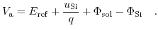
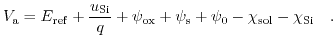
Figure 5.5:
Potential profile in an ISFET structure for a cut along the z-axis.
 The potential drop at the electrode-electrolyte interface, caused by the Gouy-Chapman-Stern double layer (
 ).
).
 The Gouy-Chapman-Stern double layer at the electrolyte-insulator
interface (
The Gouy-Chapman-Stern double layer at the electrolyte-insulator
interface ( ).
).
 The potential drop in the insulator (
 ).
).
 The potential drop due to the depletion charges in the semiconductor (
 ).
).
|
Fig. 5.5 depicts a simplified diagram for the potential profile of an ISFET structure [16].
An ISFET consists of a regular MOSFET, possessing source, drain and body contacts. However, as explained in Section 2.5, for a Biologically sensitive Field-Effect Transistor (BioFET)/ISFET the gate contact is detached from the dielectric and replaced by an electrolytic solution and a reference electrode. The main purpose of this structure is to provide efficient coupling between the electrolytic area with the electronic substrate. This kind of structure enables electronic sensing of chemical and biological processes[202].
One of the major characteristics of a FET device is the flatband voltage, which is a part of the threshold voltage
 in a MOSFET transistor. As derived in Appendix E., the flatband voltage
 of a MOSFET is related to the workfunction differences between the gate and the substrate materials, and to the amount of aggregated charge on the dielectric's surface and inner of the dielectric. Different circumstances can lead to a rise (or reduction) of the charges at the interface. This is reflected by the proportionality between the change in the amount of charge and the adjustment in the threshold voltage
. Small changes of charge can be sensed electrically. In the case of a correlation between a chemical or biological process and the modulation of charge, the ongoing process can be detected with high efficiency[203].
of a MOSFET is related to the workfunction differences between the gate and the substrate materials, and to the amount of aggregated charge on the dielectric's surface and inner of the dielectric. Different circumstances can lead to a rise (or reduction) of the charges at the interface. This is reflected by the proportionality between the change in the amount of charge and the adjustment in the threshold voltage
. Small changes of charge can be sensed electrically. In the case of a correlation between a chemical or biological process and the modulation of charge, the ongoing process can be detected with high efficiency[203].
By analogy to the analysis of a MOSFET, the bare ISFET has to be described via equations relating the occurring current in the channel to the applied voltages at the terminals. However, in addition a set of equations expressing the amount of immobilized charges via the appearing current, or, equivalently, the amount of immobilized charges via the observed shift in the threshold voltage, is needed[204].
In the following a one-dimensional model of the electrostatic potential distribution through the entire ISFET capacitor structure under a bias potential
 is derived. There are several distinctive potential drops in the structure:
- The potential drop caused by the Gouy-Chapman-Stern double layer at the electrode-electrolyte interface.
- The potential drop caused by the Gouy-Chapman-Stern double layer at the electrolyte-insulator interface.
- The potential drop within the insulator.
- The potential drop caused by the depletion of charges in the semiconductor.
Fig. 5.5 shows the electrostatic potential difference occurring due to the charge diffusion driven by the differences in work functions. Due to the insulator, there is no current flowing through the structure under equilibrium conditions. Therefore, the potential drops between the metal and the semiconductor, and between the metal and the electrolyte, are constant and do not depend on the applied bias [205]. Additionally the potential drop from the Stern layer was conjoined with the potential drop across the electrolyte, shown in Fig. 5.5. For a given bias
5.4, the following electrochemical equilibrium equation arises [204]:
 |
(5.22) |
Here,
 and
and
 denote the electrochemical potential for the metal and silicon, respectively.
 and
and
 stand for the inner potentials of the metal electrode and silicon, while
 and
and
 represent chemical potentials.
The electrostatic potential drop in the electrode-electrolyte interface is constant and independent of the applied bias under equilibrium conditions and can be merged into a reference electrode potential
represent chemical potentials.
The electrostatic potential drop in the electrode-electrolyte interface is constant and independent of the applied bias under equilibrium conditions and can be merged into a reference electrode potential
 [196]:
 |
(5.23) |
This reference potential
is fixed for a given salt concentration and a given electrode material. Substituting the definition of (5.23) into (5.22) yields:
 |
(5.24) |
The potential difference
 can be split into four different contributions:
- The diffusive double layer (also known as Gouy-Chapman layer) within the electrolyte interface ().
- The potential drop due to the depletion charge in the semiconductor (
).
- The potential drop through the dielectric (
).
- The potential drop due to the different electron affinities between the solution and the semiconductor.
Taking all these components into account leads to [203,206]:
 |
(5.25) |
Again, all constant terms can be joined in one expression, analogously to the flatband voltage in a regular MOSFET structure,
 |
(5.26) |
Without parasitic charges and defects, the externally applied potential
in the ISFET and the accumulated potential drop in the electrolyte and the semiconductor can be related via:
 |
(5.27) |
In comparison to the standard MOSFET description, there is an extra entry contributing to the overall potential drop across the structure. This potential drop is a function of the applied bias and cannot be merged into the flatband voltage. It represents the chemical and biological processes at the insulator-electrolyte interface and every biological or chemical reaction will be reflected by a modification of the potential drop .
Assuming a constant applied bias, a modulation in the potential drop will cause an adjustment in the semiconductor surface potential
and in the dielectric potential drop
, in a way consistent with (5.27). Accordingly the conductance of the channel will be modulated and a change in the source to drain current will be observed.
The three potential drops in (5.27) must be linked via two complementary conditions, in order to solve the equation system for the ISFET. One of these constraints is the charge neutrality for the whole device:
 |
(5.28) |
Supposing, there are no other charges in the system, the charges in the semiconductor side must be equal to the total charge of the double layer. The semiconductor charge is related to the surface potential by (7.39), see Appendix D., while the electric double layer charge relation (7.28) is derived in Appendix C.. Finally, the last condition is gained by the electric displacement field at the two insulator boundaries. This boundary condition demands a continuous and equal flux density at both insulator surfaces:
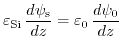 |
(5.29) |
Combining the expression for the first derivative in Appendix D. and the expression for the second derivative in Appendix C., a third equation is gained, linking the potentials ,
, and
. These three equations can be solved self-consistently (by e.g. an iterative method), and the potential distribution and channel resistance can be determined.
If the modeled system exhibits a surface with dangling bonds able to bind hydrogen, the site-binding model (5.21) has to be taken into account. Accordingly, (5.28) has to be modified to (5.22), so that the charge accumulation due to the open oxide bonds is included.
Footnotes
- ...
5.4
- between the reference electrode and the bulk contact
Next: 5.8 The ISFET as
Up: 5. Modeling of Electrolytic
Previous: 5.6 Site-Binding Model
T. Windbacher: Engineering Gate Stacks for Field-Effect Transistors
![\includegraphics[width=0.8\textwidth]{figures/potential_drops_ISFET.ps}](img775.png)