Chapter 7
Relaxation of Negative/Positive BTI
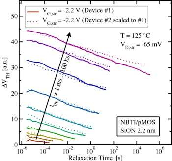
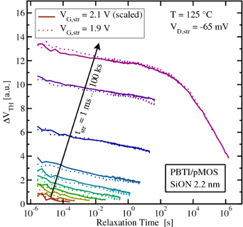
As the time constant distribution of the microscopic defects behind BTI turn out
to be a key issue, the apparent differences in relaxation behavior of negative and
positive BTI (NBTI and PBTI) on pMOSFETs, as depicted in Fig. 7.1, are now
examined under that perspective.
Although PBTI on pMOSFETs is not regarded as technologically important
as NBTI, it provides a valuable probe of the underlying physical degradation
mechanism. The most intriguing observation is that both negative and
positive bias stress create positive charges in the oxide [30], which was
already demonstrated in Chapter 4.2. However, so far the NBTI and PBTI
stress conditions were only compared in a qualitative way, i.e. strong
inversion was usually opposed to strong accumulation with undetermined
specifications concerning the exact gate voltages or oxide electric fields
applied.
For a quantitative analysis of the recovery following NBTI and PBTI
stress, long stress times  between
  and
and  are essential. The
same technology (
are essential. The
same technology ( -
- -pMOSFET) as used in Chapter 6 was
compared by the fast-
-pMOSFET) as used in Chapter 6 was
compared by the fast- method of [15] using three different oxide
thicknesses (
method of [15] using three different oxide
thicknesses ( and
and  ) and the corresponding
geometries of
) and the corresponding
geometries of  and
and  at
a constant temperature of
at
a constant temperature of  . Depending on the oxide thickness
the same applied stress voltage causes a totally different oxide electric
field. This is due to capacity of the MOSFET with its principle already
explained in Chapter 2.6. The resulting electric field at the surface of the
semiconductor
. Depending on the oxide thickness
the same applied stress voltage causes a totally different oxide electric
field. This is due to capacity of the MOSFET with its principle already
explained in Chapter 2.6. The resulting electric field at the surface of the
semiconductor  can be experimentally estimated by using the following
relation:
can be experimentally estimated by using the following
relation:
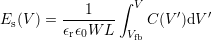 | (7.1) |
where  denotes the capacity of the MOSFET,
  the flatband voltage,
and
the flatband voltage,
and  and
and  the width and length of the device. The
  -characteristics
and the corresponding electric field are shown in Fig. 7.2 for the different device
geometries with a constant flatband voltage of
-characteristics
and the corresponding electric field are shown in Fig. 7.2 for the different device
geometries with a constant flatband voltage of  . From this figure it can
further be seen that in addition to the nonzero flatband voltage the electric field
during NBTI and PBTI is not symmetric. To create comparable degradation
conditions (not comparable degradation shifts) for both NBTI and PBTI, the
same effective field is of interest, i.e. the same magnitude, but opposite sign.
Based on the experimental
. From this figure it can
further be seen that in addition to the nonzero flatband voltage the electric field
during NBTI and PBTI is not symmetric. To create comparable degradation
conditions (not comparable degradation shifts) for both NBTI and PBTI, the
same effective field is of interest, i.e. the same magnitude, but opposite sign.
Based on the experimental  -characteristics in Fig. 7.2 the required
stress voltage
-characteristics in Fig. 7.2 the required
stress voltage  can be obtained for both NBTI and PBTI. As
an example, to achieve an
can be obtained for both NBTI and PBTI. As
an example, to achieve an  for
for  gate
voltages of
gate
voltages of  for PBTI and
  for NBTI have to be
applied.
for NBTI have to be
applied.
 . Note that degradation data
obtained with equal absolute values of the oxide electric field are compared
here.
. Note that degradation data
obtained with equal absolute values of the oxide electric field are compared
here. 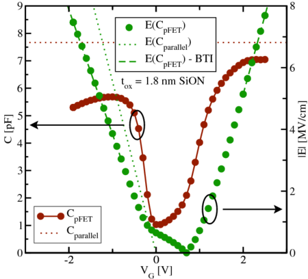
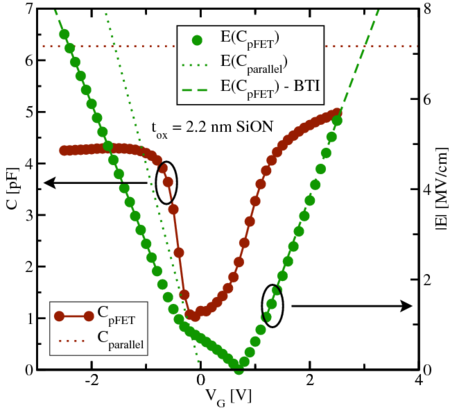
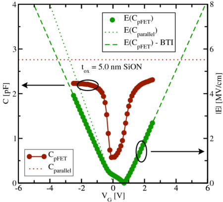
 -characteristics. Larger area devices with a
  have to be used to get satisfactory signal-to-noise ratios. The three oxide
thicknesses are
have to be used to get satisfactory signal-to-noise ratios. The three oxide
thicknesses are  (
( (
( (
( of
of  was used to
calculate the oxide electric fields
was used to
calculate the oxide electric fields  , using a flatband voltage of
  .
The capacitance of the limiting case of an ideal parallel plate capacitor of
the same thickness is plotted for comparison.
.
The capacitance of the limiting case of an ideal parallel plate capacitor of
the same thickness is plotted for comparison. 