« PreviousUpNext »Contents
Previous: 6.2 Effect of light on MIS structures Top: 6 Opto-electrical characterization of defects Next: Conclusions
6.3 Effect of light on GaN/AlGaN MIS–HEMTs
In this section we present the DLOS investigations on fully processed GaN/AlGaN MIS–HEMTs, the challenges that we have found, the solutions and the first results. The main problem has been the shielding effect of the thick aluminum gate contact, which prevented the light to properly illuminate the device. For this reason, new test structures have been fabricated choosing a more suitable material and realizing a the thinnest layer possible for contacting. Finally, we report and interpret the DLOS spectra measured on the new devices.
6.3.1 DLOS on standard MIS–HEMTs
Our goal with the DLOS experiment is to characterize the defect levels with large activation energy present in our devices, and try to understand the impact of the defects at the AlGaN/SiN interface. In order to do so, we compare the DLOS spectra with and without a filling pulse at positive gate voltage. As we have discussed in the previous chapters, applying a forward gate bias results in electron trapping at the interface we are interested in. With the DLOS experiment we are going to evaluate the impact of light on the recovery from such a stress. We must note that, due to the broad distribution of time constants, we would always observe a combination of thermal and optical emission, at all temperatures and during the whole transient. However, we are going to analyze the recovery transients with the method described in Section 6.1.1 and extract the spectral response of our test structures under different values of recovery voltage.
In the first place, we must take into account that the application of any read out voltage different from zero results in a  drift of the device (see the description of the
hysteresis effect in Section 3.2.2). The challenging feature is that the drift would be different when the same stress/recovery pattern is used more than once (see again Fig. 3.15b). This is problematic for the DLOS experiment because we need to repeat the filling pulse and the recovery for all different values of light energy in order to have a
well–resolved spectrum. The solution used here is to repeat ten times a full sweep of gate voltage from depletion to 0 V, until the voltage shift approaches saturation. In this way, the conditions of the devices are always approximately the same at the
beginning of every cycle of stress/recovery.
drift of the device (see the description of the
hysteresis effect in Section 3.2.2). The challenging feature is that the drift would be different when the same stress/recovery pattern is used more than once (see again Fig. 3.15b). This is problematic for the DLOS experiment because we need to repeat the filling pulse and the recovery for all different values of light energy in order to have a
well–resolved spectrum. The solution used here is to repeat ten times a full sweep of gate voltage from depletion to 0 V, until the voltage shift approaches saturation. In this way, the conditions of the devices are always approximately the same at the
beginning of every cycle of stress/recovery.
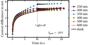
Figure 6.5: I–DLOS transients of the standard GaN/AlGaN/SiN MIS–HEMTs at a read out voltage of −20 V, in dark conditions and under exposure to monochromatic light. The initial value of current is subtracted for better comparison. Unfortu- nately, the difference between the various photon energies used is very small.
We measure the drain current of the MIS–HEMTs, performing the so–called current–DLOS (I–DLOS) experiment. We apply a constant voltage between the drain and the source contact of 2 V. The recovery transients are shown in Fig. 6.5 for a read out voltage of −20 V, which is one of the gate bias points where the effect of the light is largest. Unfortunately, we observe that the impact of light is much smaller than that of the drift due to the applied gate bias. In fact, only the curve at 350 nm, the one matching the energy of the bandgap, results in a clear increase of drain current with respect to the transient measured in dark conditions. As a consequence, the extraction of the optical cross section gives a very poor and noisy spectrum. The cause has been found to be the thick aluminum contact on top of the active area, which almost entirely absorbs the optical radiation. For this reason, we prepared new test structures dedicated to experiments with light, as presented in the next section.
6.3.2 Thin gold contacts on MIS–HEMTs for optical characterization
A proper choice of the metal to realize the top contact can be made after evaluating the absorption coefficient,  , of the material. According to the Beer–Lambert law, the intensity of an electromagnetic
wave propagating in a medium decays as
, of the material. According to the Beer–Lambert law, the intensity of an electromagnetic
wave propagating in a medium decays as

where  is the distance and depends linearly on the extinction coefficient
  , i.e., the imaginary part of the complex reflective index.
Fig. 6.6 shows the absorption coefficient of aluminum, gold and titanium as a function of the photon wavelength. As we can see, is almost one order of magnitude larger for aluminum with respect to the other two metals.
In fact, Al is one of the most reflecting materials and is used to make the gratings of monochromators, where maximum reflectance over a broad range of wavelengths is required. On the other hand, gold and titanium are both good choices to realize a gate contact
that could transmit part of the optical radiation to the device underneath.
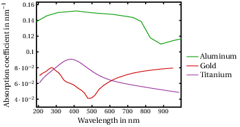
Referring to monochromatic light with a wavelength of 350 nm, we can calculate the ratio between the intensity of the incident light and that after 1 nm of metal in the three cases. The results are reported in Table 6.1.


While gold and titanium let through more than 90% of the incident light, for aluminum the percentage is 85%. A layer of aluminum 50 nm thick is already enough to bring the percentage of transmitted light to lower than 1%. It is therefore clear that our first devices, featuring several hundreds of nanometers of aluminum on top, are not the ideal test structures for optical investigations. The impact of light we measured in the previous section is probably due to the very small SiN area that is not covered by the gate.
The gate contact of the new test structures has been realized by evaporation of gold and, to ensure a better adhesion to the SiN, with an additional layer of titanium between the gold and the AlGaN. Four wafers with different layer thicknesses have been fabricated, summarized in Table 6.2 together with the estimate of the transmitted to incident light ratio at 350 nm.
Most of the devices on all wafers can be successfully contacted with the needles of the probe station, even though care must be taken in the process. The device to device variation in the contact quality is quite large, giving rise to a variation in the saturation drain current measurement that can reach 20%. However, we can use a single test structure for a full DLOS experiment. In fact, we perform a series of ten identical voltage sweep between every read out transient under exposure, which enables us to bring the device always to the same conditions prior to the measurement.
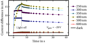
The transients measured at a read out voltage of −20 V are shown in Fig. 6.7. By comparison with Fig. 6.5, it is clear that the effect of light on the new structures is much larger. This allows the proper execution of I–DLOS investigations, that are the object of the next section.
6.3.3 DLOS on MIS–HEMTs with thin gold contacts
The large impact of light on the I–DLOS transients allows us to extract the spectral response of the device, which is directly proportional to the optical cross section. In general, we obtain an increase of the spectral response with the photon energy, with few clear “shoulders” that can be fitted with the Lucovsky model. The energy range of our setup goes from 2 eV to about 5 eV, which is still below the 6.2 eV bandgap of the SiN material.
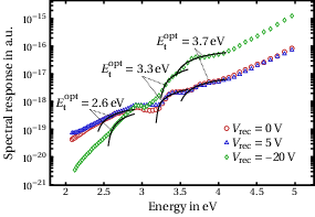
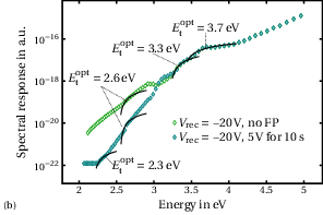
Fig. 6.8 shows the result of the I–DLOS experiment without the positive bias filling pulse, at the read out voltages of 0 V, 5 V (spill–over conditions) and −20 V (depletion conditions). The shape of the spectral response at 0 V and 5 V is basically the same. We can distinguish three trap–related “shoulders”. At −20 V we see the same trap levels, but the magnitude of the one at low energy is larger. Since the measurement in depletion is the most sensitive to buffer traps, these defects are probably located in the GaN bulk.
The three states have optical activation energies of 2.6 eV, 3.3 eV and 3.7 eV. The defect with  2.6 eV has been measured
extensively in literature, as well as in the carbon–doped samples in Section 6.1.2, and it is usually related to the gallium vacancy in the GaN buffer [105]. The level at 3.3 eV is also often observed in MOCVD grown structures and is likely due to the
carbon substitutional defect in the GaN [105, 106]. The last trap state at energy 3.7 eV might be located in the AlGaN layer. In fact, its origin has been suggested to be the carbon substitutional defect in the AlGaN
material [35, 106].
2.6 eV has been measured
extensively in literature, as well as in the carbon–doped samples in Section 6.1.2, and it is usually related to the gallium vacancy in the GaN buffer [105]. The level at 3.3 eV is also often observed in MOCVD grown structures and is likely due to the
carbon substitutional defect in the GaN [105, 106]. The last trap state at energy 3.7 eV might be located in the AlGaN layer. In fact, its origin has been suggested to be the carbon substitutional defect in the AlGaN
material [35, 106].
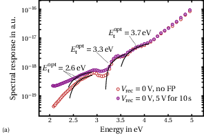
We investigate the effect of a filling pulse at positive gate bias, namely 5 V for 10 s. When the read out voltage is 0 V, the difference with and without filling pulse is just a slight modification of the spectrum at low energy, around 2 eV, as shown in Fig. 6.9a. However, this is indeed too small to perform a Lucovsky fit. The other three states at 2.6 eV, 3.3 eV and 3.7 eV are still present.
In depletion conditions, the presence of the filling pulse results in a clearer additional level at low energies. The fit to the data in Fig. 6.9b suggests a trap with optical activation energy of 2.3 eV. Such a defect has been measured previously [105, 106], and it has been related to the access region when a SiN passivation is used. Under this assumption, this would be the fingerprint of a defect state at the AlGaN/SiN interface. The fact that this level arises only when a filling pulse at forward gate bias is used confirms this hypothesis.
In conclusion, the I–DLOS experiment has been successfully performed on structures with a thin gold gate contact, allowing the extraction of the optical energy of several active trap levels. The comparison of the spectra at various read out biases and after different filling pulses can aid the identification of the defects, as well as their location inside the device.
« PreviousUpNext »Contents
Previous: 6.2 Effect of light on MIS structures Top: 6 Opto-electrical characterization of defects Next: Conclusions