« PreviousUpNext »Contents
Previous: 4 Modeling of charge trapping phenomena Top: 4 Modeling of charge trapping phenomena Next: 4.3 Extraction of the activation energy and from experimental data
4.2 The non–radiative multiphonon (NMP) model
A model capable of describing the physical mechanisms of charge exchange cannot ignore the structural deformation at the defect site. In fact, after an electron (or hole) is captured (or emitted) the microscopic configuration of the defect and the surrounding
area changes into a different arrangement. Bond lengths and angles are adjusted in order to accommodate the captured (or missing) charge. In other words, the whole system relaxes towards its new equilibrium position, which is defined by the total potential
energy of the system in the respective charge state. The total potential energy is often approximated by a harmonic potential. The equilibrium configuration is therefore defined by a certain equilibrium position  (representing the mass–weighted coordinates of the defect
site) and a certain equilibrium energy
(representing the mass–weighted coordinates of the defect
site) and a certain equilibrium energy  , corresponding to the minimum of the harmonic potential. This is illustrated in Fig. 4.2.
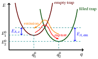
Figure 4.2: The potential energy of a defect site is approximated by a harmonic potential, which takes different equilibrium positions depending on its charge state. A charge exchange event is
therefore a transition between the two potential energy surfaces. In the classical limit, a non–radiative, multiphonon transition must occur through their crossing point, as shown by the arrows.
When a trapping (or detrapping) event takes place, the equilibrium position and the energy of the system change. In this way, the transition from the initial state in  to the final state in
  requires a transition between two potential energy
surfaces. Without any external electromagnetic excitation, in a classical, high temperature approximation this can happen only through the crossing point of the two potential energy functions. In this way, an energy barrier is associated with each charge trapping
event. The excess energy, called activation energy
requires a transition between two potential energy
surfaces. Without any external electromagnetic excitation, in a classical, high temperature approximation this can happen only through the crossing point of the two potential energy functions. In this way, an energy barrier is associated with each charge trapping
event. The excess energy, called activation energy  , is provided to the system as thermal energy through
phonon scattering. A non–radiative multiphonon (NMP) transition [76–78] is therefore a thermally activated process, which can be described in the classical high–temperature limit by the Arrhenius equation
, is provided to the system as thermal energy through
phonon scattering. A non–radiative multiphonon (NMP) transition [76–78] is therefore a thermally activated process, which can be described in the classical high–temperature limit by the Arrhenius equation

We note the similarity of Eq. (4.3) with Eq. (4.2), if we assume  (or
(or  ). The difference is the physical meaning of the energetic barrier: in the SRH picture, it is defined by the energetic position of the trap with respect to the reservoir; for the NMP model it must be determined from the shape and
position of the potential energy functions of the initial and final defect configurations.
). The difference is the physical meaning of the energetic barrier: in the SRH picture, it is defined by the energetic position of the trap with respect to the reservoir; for the NMP model it must be determined from the shape and
position of the potential energy functions of the initial and final defect configurations.
The temperature dependence of a charge trapping event is given by the Boltzmann factor in the Arrhenius equation, while the applied bias has an influence on the activation energy. In fact, a modification to the gate voltage results in an offset for one of the two
potential energy surfaces, thereby changing their relative positions and thus causing a different .
With such a picture of the trapping mechanism we are able to explain very complex charge trapping dynamics, which would not be possible with the model presented in the previous section. For example, the physical model based on NMP transition can
explain complex CET maps, allowing a defect to have a short time constant for capture but a long one for emission, because it is possible to find a state with a low barrier energy for capture and a large one for emission processes [79]. In fact, some defects have
similar capture and emission time constants and therefore can be charged and discharged continuously within stress and recovery cycles, resulting in a fully recoverable degradation. Other trap sites have emission times much longer than for capture, giving rise to
an almost permanent voltage drift, which can eventually recover only after very long time, or with high temperature annealing processes. Furthermore, it was shown that the behavior of threshold voltage drifts of silicon MOSFETs under NBTI can be fully
explained only introducing intermediate, metastable defect configurations between the empty trap equilibrium state  and the filled trap equilibrium state
  [80]. These states can be represented in
our picture as local minima of the potential energy surfaces, with very similar energy values. The metastable states are also responsible for the anomalous random telegraph noise (RTN) observed in such structures [27, 81].
[80]. These states can be represented in
our picture as local minima of the potential energy surfaces, with very similar energy values. The metastable states are also responsible for the anomalous random telegraph noise (RTN) observed in such structures [27, 81].
The temperature dependence of Eq. (4.3) can be used for temperature acceleration [82, 83]. Each experimental
dataset is conducted at constant temperature (isothermal measurements), and we expect the trap sites to contribute to the device drift in a different way at different temperatures. However, the time constants  and
and  of the same defect at temperature
  and
and  are related to each other by

where  is the coefficient of the Arrhenius’ equation.
Eq. (4.4) enables us to bring all measurements at different temperature on the same axis, by introducing the
temperature–time variable
is the coefficient of the Arrhenius’ equation.
Eq. (4.4) enables us to bring all measurements at different temperature on the same axis, by introducing the
temperature–time variable

This means that a measurement at cold temperature in the time window between  and
and  is equivalent to a measurement at higher temperature
between
is equivalent to a measurement at higher temperature
between  and
and  . In other words, temperature has the effect of
accelerating both stress and recovery mechanisms. This allows us to fix our experimental time window, and investigate shorter time scales by using low temperatures, and longer time scales by increasing it. The shortest accessible time is therefore determined by
two factors: the time resolution of the instrument and the coldest temperature achievable in our setup.
. In other words, temperature has the effect of
accelerating both stress and recovery mechanisms. This allows us to fix our experimental time window, and investigate shorter time scales by using low temperatures, and longer time scales by increasing it. The shortest accessible time is therefore determined by
two factors: the time resolution of the instrument and the coldest temperature achievable in our setup.
In the following, we examine three different scenarios of increasing complexity. The simplest case is to consider a constant parameter and to be single–valued (Section 4.2.1). However, this
approximation can be too rough to properly explain the experimental data. Therefore, we consider the possibility of a continuous distribution of activation energies in Section 4.2.2, and of a non constant in Section 4.2.3.
4.2.1 Constant  , single activation energy
In general, under certain bias conditions, every defect has different parameters and . However, in a first approximation we can consider the
pre–factor to be constant. This has been proven to be accurate
enough for NBTI investigations on silicon MOSFETs [83]. Furthermore, we can recognize “families” of states, or defects of the same type, that have approximately the same activation energy. For example, we can group in a “family” all defects that have the same
microscopic configuration (due to a certain impurity), or the same origin (due to the vacancy of a certain element). In this way, the charge trapping mechanisms are described by Eq. (4.3) with a constant factor and one, or more in case there are more defect
“families”, single–valued activation energies.
According to the Arrhenius equation, the time response of every single interface state follows an exponential function with characteristic time  . Each defect type
  , with activation energy
  , gives rise to the time constant
  , and contributes to the total voltage shift of the device
with the fraction
, and contributes to the total voltage shift of the device
with the fraction  . Summing up over all contributions, and
assuming that electrons are being trapped into defects during stress, the threshold voltage shift increases as
. Summing up over all contributions, and
assuming that electrons are being trapped into defects during stress, the threshold voltage shift increases as

and then, after it reaches a maximum threshold voltage shift of  , recovers according to

If the activation energies of the defect types are quite different, it is possible to distinguish each contribution directly by looking at the time evolution of the  [18]. The various and the respective can be easily extracted from a fit to the data. In
Section 4.3.1 we present a straightforward method to extract the activation energy from
[18]. The various and the respective can be easily extracted from a fit to the data. In
Section 4.3.1 we present a straightforward method to extract the activation energy from  data measured at different temperatures.
4.2.2 Constant  , distributed activation energy
Experimental evidence has shown that the single exponential model is normally not sufficient to explain the actual time evolution of  . In fact, we should consider that the interface between two materials, especially in the case
of an amorphous dielectric, is characterized by a certain amount of variability in the arrangement of the atoms. For this reason, also the defects exhibit a certain diversity in bond length and angles, thus resulting in a continuous interval of allowed activation
energies rather than a precise, single value . For example, we can describe a defect “family” with
a gaussian distribution of activation energies around a mean value
. In fact, we should consider that the interface between two materials, especially in the case
of an amorphous dielectric, is characterized by a certain amount of variability in the arrangement of the atoms. For this reason, also the defects exhibit a certain diversity in bond length and angles, thus resulting in a continuous interval of allowed activation
energies rather than a precise, single value . For example, we can describe a defect “family” with
a gaussian distribution of activation energies around a mean value  , with a certain standard deviation
  . As a consequence, capture and emission time constant will follow a log-normal
distribution and an analytical expression for the device drift can be written as [79]
. As a consequence, capture and emission time constant will follow a log-normal
distribution and an analytical expression for the device drift can be written as [79]

for stress, and

for recovery, where  is the voltage drift at saturation,
achieved when all traps have been filled. This approach contributed to great advances in the understanding of the defects present at Si/SiO
is the voltage drift at saturation,
achieved when all traps have been filled. This approach contributed to great advances in the understanding of the defects present at Si/SiO interfaces and responsible for NBTI: here two main
“families” of trap states with gaussian–distributed activation energies have been discovered [27].
interfaces and responsible for NBTI: here two main
“families” of trap states with gaussian–distributed activation energies have been discovered [27].
However, the problem of determining the relevant defect groups from the experimental data may be complex if we observe a large number of contributions with very close values. This is exactly the case for standard GaN/AlGaN
MIS–HEMTs, for which a logarithmic temporal evolution is observed [47, 67]. In fact, a function  can be fitted only by a large
number of exponential components of the kind
can be fitted only by a large
number of exponential components of the kind  . The fit of a dataset constituted by a
finite number of points,
. The fit of a dataset constituted by a
finite number of points,  , with a multi–exponential model with an unknown number
  of exponential components is in fact an ill–posed problem [84]. The system in
this case is underdetermined: this means that a set of solutions exists, rather than a unique one. A regularization method is therefore necessary in order to find the solution. If no additional information about the system is known, different approaches
can be used. For example, the Tikhonov regularization method [84] solves the problem by adding a constraint given by a certain smoothing functional of the solution. The method of maximum entropy (MEM) [85, 86] instead chooses the
most noncommital solution, i.e., the one which makes the least assumption on the data, thus fulfilling the parsimony principle by maximizing the Shannon entropy [87]. In our case, we can apply a method that has been developed for the investigation of
chemical reactions involving distributed activation energies, which is described in Section 4.3.2.
of exponential components is in fact an ill–posed problem [84]. The system in
this case is underdetermined: this means that a set of solutions exists, rather than a unique one. A regularization method is therefore necessary in order to find the solution. If no additional information about the system is known, different approaches
can be used. For example, the Tikhonov regularization method [84] solves the problem by adding a constraint given by a certain smoothing functional of the solution. The method of maximum entropy (MEM) [85, 86] instead chooses the
most noncommital solution, i.e., the one which makes the least assumption on the data, thus fulfilling the parsimony principle by maximizing the Shannon entropy [87]. In our case, we can apply a method that has been developed for the investigation of
chemical reactions involving distributed activation energies, which is described in Section 4.3.2.
4.2.3 Non–constant
In the cases discussed until now, the pre–factor is assumed to be constant, to be determined as a
parameter of the fit to the whole dataset of measurements taken at different temperatures. However, in certain cases this approximation can be too crude and might lead to an error in the determination of the activation energy values.
The physical meaning of for a single charge transfer reaction following
Eq. (4.3) can be related to the phonon frequency, i.e., how many phonons per unit time are available to provide energy to
overcome the energetic barrier. In fact, the fitted value of from investigations on silicon MOSFETs agrees with
the inverse of the phonon frequency in silicon, which has been measured and can be estimated with DFT calculations to be on the order of 1013 Hz [83].
The first reason for the failure of the constant approximation can be a large variety of defect types.
In fact, each type would have a characteristic  for its charge exchange reaction, related to the
attempt frequency in that particular case. Such is already an approximated value, averaged
over the entire “family” of similar defects, each of which has its own characteristic . The overall effect on a macroscopic device, however,
has a characteristic time constant given by the average over the of all the active defects in those conditions. As
a consequence, if measurements at different temperatures access different defect types, it is clear that a single cannot be found. For example, this can happen if
some traps have a quite large time constant, becoming active only at high temperatures, but are not accessible at low temperatures. The whole dataset from low to high temperatures in this case cannot be fitted accurately with the same . An experimental approach that allows to avoid this
problem is the time–dependent defect spectroscopy (TDDS), developed and used for NBTI studies on Si/SiO MOSFETs. It relies on the measurement of small–area
devices, thus allowing to deal with only a handful of defects at a time [80, 88, 89] and therefore to determine the properties of each trap state individually.
for its charge exchange reaction, related to the
attempt frequency in that particular case. Such is already an approximated value, averaged
over the entire “family” of similar defects, each of which has its own characteristic . The overall effect on a macroscopic device, however,
has a characteristic time constant given by the average over the of all the active defects in those conditions. As
a consequence, if measurements at different temperatures access different defect types, it is clear that a single cannot be found. For example, this can happen if
some traps have a quite large time constant, becoming active only at high temperatures, but are not accessible at low temperatures. The whole dataset from low to high temperatures in this case cannot be fitted accurately with the same . An experimental approach that allows to avoid this
problem is the time–dependent defect spectroscopy (TDDS), developed and used for NBTI studies on Si/SiO MOSFETs. It relies on the measurement of small–area
devices, thus allowing to deal with only a handful of defects at a time [80, 88, 89] and therefore to determine the properties of each trap state individually.
A second reason for a non–constant can be found in the inaccuracies arising from the
classical approximation. In fact, Eq. (4.3) is based on the assumption that a transition between two potential energy functions
occurs at the intersection point (IP), as illustrated in Fig. 4.3a. The IP determines the height of the barrier, that is the activation energy . However, the quantum–mechanical approach to the same
problem possibly leads to a lower value for the energy barrier and a different . The solutions of a harmonic potential are
wavefunctions characterized by a discrete energy spectrum, as shown in Fig. 4.3a. Depending on the distance of the two equilibrium positions and , it can happen that some excited states of the two
harmonic potentials overlap at an energy below that of the IP. This gives a certain probability for the transition at a lower energy barrier than the classical one through carrier tunnelling. In Fig. 4.3b the activation energy in the classical limit and with the quantum–mechanical approach have been calculated as a function of temperature and for different values of
displacement  [90], performing density
functional theory (DFT) calculations based on the data obtained by TDDS studies on silicon MOSFETs. The error on due to tunnelling is larger at cold temperatures, and it can
be still relevant under typical conditions of device operation (down to 300 K). Unfortunately, at the present time it is not yet possible to perform the same calculations for GaN/AlGaN MIS–HEMTs, since the properties of the defects needed for DFT
simulations are still unknown. Further investigations and the improvement of the characterization methods are therefore necessary to clarify this aspect.
[90], performing density
functional theory (DFT) calculations based on the data obtained by TDDS studies on silicon MOSFETs. The error on due to tunnelling is larger at cold temperatures, and it can
be still relevant under typical conditions of device operation (down to 300 K). Unfortunately, at the present time it is not yet possible to perform the same calculations for GaN/AlGaN MIS–HEMTs, since the properties of the defects needed for DFT
simulations are still unknown. Further investigations and the improvement of the characterization methods are therefore necessary to clarify this aspect.
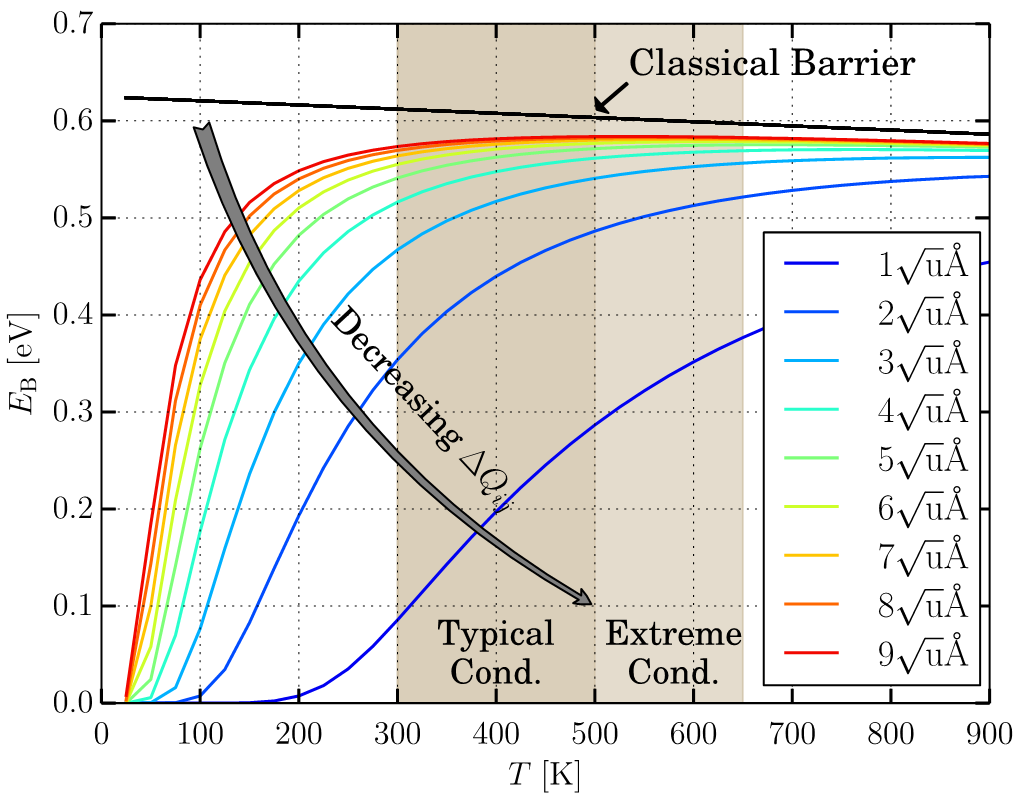

Figure 4.3: The transition between two potential energy surfaces occurs at the intersection point (IP) in the classical approximation, but in the quantum–mechanical approach tunnelling between two wavefunctions can take place as well (a). The resulting
activation energy can be much lower than the classical value (b), depending on temperature and the displacement  between the two equilibrium coordinates (from
[90]).
between the two equilibrium coordinates (from
[90]).
In conclusion, if the wavefunction overlap is not negligible, the extraction of and with Eq. (4.3) results in non–constant, temperature–dependent values: at higher temperature the energy would increase while would decrease. We discuss further the possible
effects of a non–constant in Section 4.3.3.
Previous: 4 Modeling of charge trapping phenomena Top: 4 Modeling of charge trapping phenomena Next: 4.3 Extraction of the activation energy and from experimental data