« PreviousUpNext »Contents
Previous: 3 Methodologies for electrical characterization of interface defects in GaN-based MIS-HEMTs Top: 3 Methodologies for electrical characterization of interface defects in GaN-based MIS-HEMTs Next: 3.3 Voltage shift methods
3.2 Impedance characteristics of GaN/AlGaN MIS structures
In this section, we focus on the two reasons why the main established methods are not adequate for our GaN/AlGaN MIS devices. In the first place, we investigate the role of the barrier, developing a new equivalent circuit model that can explain the observed frequency dispersion. Furthermore, we study in more detail the dependence of the impedance characteristics on the measurement parameters and the hysteresis of the devices with the standard interface.
3.2.1 The role of the AlGaN barrier
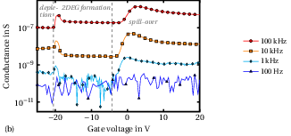
The study of the impedance characteristics of a composite GaN/AlGaN structure allows us to obtain an accurate insight into the different regions of operation of the device and its frequency response. As we can see in Fig. 3.13, from the capacitance– and conductance–voltage curves we can distinguish three main regions, indicated as depletion, 2DEG formation and spill–over.
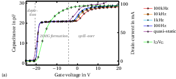

When the gate bias is more negative than the threshold voltage,  , around −20 V in Fig. 3.13, the electrons of the 2DEG are pushed away from the GaN/AlGaN interface. This results in the creation of a depletion region, which extends in the semiconductor
according to its doping profile. Since the generation time constant for holes is very large in wide bandgap materials, there are not enough minority carriers to form an inversion layer. As a consequence, at further negative gate voltages we never measure a constant
inversion capacitance value, but we we are in deep depletion conditions.
, around −20 V in Fig. 3.13, the electrons of the 2DEG are pushed away from the GaN/AlGaN interface. This results in the creation of a depletion region, which extends in the semiconductor
according to its doping profile. Since the generation time constant for holes is very large in wide bandgap materials, there are not enough minority carriers to form an inversion layer. As a consequence, at further negative gate voltages we never measure a constant
inversion capacitance value, but we we are in deep depletion conditions.
Above the threshold voltage, the 2DEG is formed at the GaN/AlGaN interface. As we can see in the transfer characteristic in Fig. 3.13a, the device turns on and the
electron flow between the source and drain contacts is possible. The capacitance almost abruptly reaches the plateau value  ,
which is the result of the dielectric capacitance and that of the barrier in series. The conductance curve reflects the behavior of the displacement currents in the device. In Fig. 3.13b we can see a conductance peak in correspondence of the value, which is the point at which the electron gas
is formed.
,
which is the result of the dielectric capacitance and that of the barrier in series. The conductance curve reflects the behavior of the displacement currents in the device. In Fig. 3.13b we can see a conductance peak in correspondence of the value, which is the point at which the electron gas
is formed.
At more positive gate voltages, starting from the spill–over voltage  , the capacitance increases towards
  and the conductance curve has another peak.
This means that the electrons from the 2DEG found their way to through the AlGaN barrier to the interface with the dielectric.
and the conductance curve has another peak.
This means that the electrons from the 2DEG found their way to through the AlGaN barrier to the interface with the dielectric.
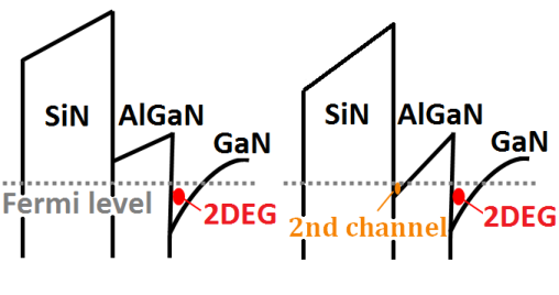

In fact, starting from the spill–over voltage, the edge of the conduction band at the AlGaN/dielectric interface is brought below the Fermi level, as shown in Fig. 3.14a. This results in the creation of a second electron channel. Interestingly, the AlGaN layer, which has a purely capacitive behavior below , for more positive gate bias becomes conductive,
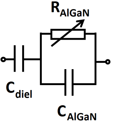
thus allowing for electron transport from one side to the other. The GaN/AlGaN/dielectric structure can therefore be described by the circuit model in Fig. 3.14b,
the dielectric capacitance in series with a parallel circuit of  and the bias–dependent barrier resistance,
 . Such an RC circuit responds to a
small–signal excitation in a frequency dependent way. As a consequence, this trap–free model can already explain the frequency dispersion observed in Fig. 3.13,
and the frequency dependence of the spill–over voltage. It is possible to reproduce the experimental data by fitting the barrier resistance as a function of the gate bias [46].
. Such an RC circuit responds to a
small–signal excitation in a frequency dependent way. As a consequence, this trap–free model can already explain the frequency dispersion observed in Fig. 3.13,
and the frequency dependence of the spill–over voltage. It is possible to reproduce the experimental data by fitting the barrier resistance as a function of the gate bias [46].
The observed spill–over voltage in impedance measurements also depends on the frequency used. The lower the frequency, the smaller appears. In fact, the low frequency limit ( ) of the circuit in Fig. 3.14b is the dielectric capacitance. In this case the barrier is “short circuited” and the dominant term is . On the other hand, the high frequency limit
(
) of the circuit in Fig. 3.14b is the dielectric capacitance. In this case the barrier is “short circuited” and the dominant term is . On the other hand, the high frequency limit
( ) is the serial connection of the dielectric and the barrier
capacitances, which explains the lower values of measured capacitance at high frequencies. For this reason, the most accurate way to determine the spill–over voltage is the quasi–static CV method: we directly measure the displacement current in the MIS
structure by applying a small, linear increase of gate voltage. The incremental capacitance is proportional to the measured current. In order to calculate the capacitance of the device, we subtract the leakage current and integrate the result over time. The
quasi–static CV curve obtained in this way is shown in Fig. 3.13a. As expected, this method provides the smallest value of the spill–over voltage. For the standard
GaN/AlGaN/SiN structures,
) is the serial connection of the dielectric and the barrier
capacitances, which explains the lower values of measured capacitance at high frequencies. For this reason, the most accurate way to determine the spill–over voltage is the quasi–static CV method: we directly measure the displacement current in the MIS
structure by applying a small, linear increase of gate voltage. The incremental capacitance is proportional to the measured current. In order to calculate the capacitance of the device, we subtract the leakage current and integrate the result over time. The
quasi–static CV curve obtained in this way is shown in Fig. 3.13a. As expected, this method provides the smallest value of the spill–over voltage. For the standard
GaN/AlGaN/SiN structures,  −4 V.
−4 V.
3.2.2 Dependence on measurement parameters
As we mentioned in Section 3.1.3, the impedance characteristics of the MIS–HEMT structures with a standard AlGaN/SiN interface show a strong dependence on the sweep rate. In this subsection we focus on the effect of the measurement parameters, varying the direction of the sweep, the oscillating amplitude, the sweep rate and the start and stop gate bias values.
By changing the direction of the sweep we investigate the hysteresis of the device characteristics. We perform a series of measurements on a number of fresh devices starting at 0 V, reaching a final gate bias value  (towards positive and negative voltages) and
returning back to zero. The results are shown in Fig. 3.15a: the first part of the sweep is along the green curves, the return sweeps are in color, blue scale for
(towards positive and negative voltages) and
returning back to zero. The results are shown in Fig. 3.15a: the first part of the sweep is along the green curves, the return sweeps are in color, blue scale for  0 V (5 V, 10 V,
15 V) and red scale for
0 V (5 V, 10 V,
15 V) and red scale for  0 V (−10 V, −20 V,
−30 V). We observe hysteresis along the whole gate bias axis, and the device status at the end of one cycle is different from fresh conditions. This can be seen clearly in the different capacitance value at 0 V before and after the hysteresis cycle with
0 V (−10 V, −20 V,
−30 V). We observe hysteresis along the whole gate bias axis, and the device status at the end of one cycle is different from fresh conditions. This can be seen clearly in the different capacitance value at 0 V before and after the hysteresis cycle with
 −30 V.
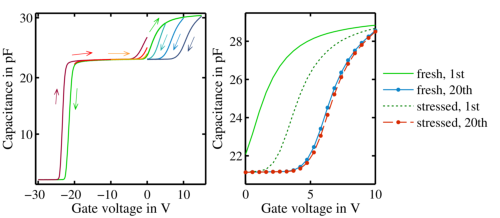

Furthermore, if we repeatedly sweep the gate bias between zero and we observe a progressive shift of the CV curve,
towards more positive voltages if  and towards more negative voltages if
 . In Fig. 3.15b we use 10 V and we switch the bias twenty
times. The curves labeled “fresh” are the first and the last sweep in the same direction, taken on a fresh device. We obtain a positive shift of about 5 V. Leaving the device floating results in a partial recovery of the voltage shift, as shown by the repetition of
this experiment on the same device after some minutes (the two curves labeled “stressed”). We also note that the final sweeps (labeled “20th”) are very similar. This means that a sort of saturation is reached, at least apparently, by repeating many times the same
gate bias sweep. However, the final position of the CV curve depends on the used, and it starts recovering as soon as the
device returns to floating conditions.
. In Fig. 3.15b we use 10 V and we switch the bias twenty
times. The curves labeled “fresh” are the first and the last sweep in the same direction, taken on a fresh device. We obtain a positive shift of about 5 V. Leaving the device floating results in a partial recovery of the voltage shift, as shown by the repetition of
this experiment on the same device after some minutes (the two curves labeled “stressed”). We also note that the final sweeps (labeled “20th”) are very similar. This means that a sort of saturation is reached, at least apparently, by repeating many times the same
gate bias sweep. However, the final position of the CV curve depends on the used, and it starts recovering as soon as the
device returns to floating conditions.
In order to understand the impact of the sweep direction in more detail, we perform the following experiment with the lock–in amplifier. We apply an increasing or decreasing gate bias sweep in a staircase pattern. This means that we hold each bias value for a
time  , and then we instantaneously switch to the
next value. From the capacitance transients at each gate voltage we extract the value at time
, and then we instantaneously switch to the
next value. From the capacitance transients at each gate voltage we extract the value at time  , and use it to build the whole CV curve. The
results for different choices of , and for positive (“up”) and negative
(“down”) sweep directions are shown in Fig. 3.16. We use a fresh device for every measurement.
, and use it to build the whole CV curve. The
results for different choices of , and for positive (“up”) and negative
(“down”) sweep directions are shown in Fig. 3.16. We use a fresh device for every measurement.
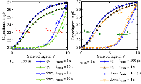

Figure 3.16: CV curves extracted from the staircase voltage pattern with the lock–in amplifier. (a) Each bias step is held for a time  1 s or 10 s, and the capacitance is always
extracted at
1 s or 10 s, and the capacitance is always
extracted at  100 µs. (b) Each step dura-
tion is 1 s and the extraction time is 100 µs or 1 s. In both cases the comparison
of the positive (up) and negative (down) sweep direction is shown (from [67]).
100 µs. (b) Each step dura-
tion is 1 s and the extraction time is 100 µs or 1 s. In both cases the comparison
of the positive (up) and negative (down) sweep direction is shown (from [67]).
Using a shorter or longer duration for each bias step has the same effect on the sweeps in different
direction, resulting in a certain positive shift for every point of the CV curve (see Fig. 3.16a). In fact, we apply only positive gate voltages, for which a positive shift
of the capacitance characteristic is observed. This is due to electron capture, and in this case the capacitance transients at every gate bias step decrease as a function of time. For this reason, even if the extraction time is always the same, the longer the device has
been at positive bias, the larger is the accumulated positive shift. This explains also the distortion of the curves when gets longer. On the other hand, using the
same but different extraction times we obtain the opposite behavior in the “up”
and “down” sweeps, as we can see in Fig. 3.16b. In the former case, we observe a decrease of capacitance as a function of time for every gate voltage step. A longer
therefore results in a larger positive shift. If
the sweep direction is negative instead, the capacitance transients increase in time, because some electron emission takes place at lower gate voltages. In this way, each bias step allows some recovery from the previous one. There are two competing effects: the
electron capture due to the application of forward gate bias, and the electron emission because of the continuous reduction of the gate voltage. As a consequence, waiting for a certain time at each bias step lets these two effects
balance each other out, thus minimizing the effect of trapping and detrapping during the measurement of the CV curve.
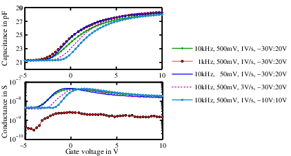
Figure 3.17: Capacitance and conductance characteristics measured with different values of frequency, oscillator level, sweep rate and start and stop voltage. Only the part from −5 V to 10 V is shown in order to focus on the differences in the spill–over region. The parameters used are indicated in the legend.
Among the measurement parameters that have an impact on the shape of the CV and conductance curves, we have discussed the frequency of the AC signal, the sweep direction and the sweep rate. Other important quantities are the oscillator level and the voltage extrema of the sweep. Fig. 3.17 compares the impedance characteristics measured with frequency 10 kHz, oscillator level 500 mV, sweep rate 1 V/s, starting from −30 V and stopping at 20 V with the curves obtained by changing one parameter at a time. We conclude that the impedance characteristics depend strongly on the measurement parameters. This is due to the fact that the structure does not reach the quasi–equilibrium conditions required to apply the small–signal approximation. This means that the trap states are not in resonance with the AC signal, capturing and emitting electrons following the oscillations, but that the DC bias itself causes a time–dependent shift of the threshold voltage, which is very sensitive to the measurement parameters listed above.
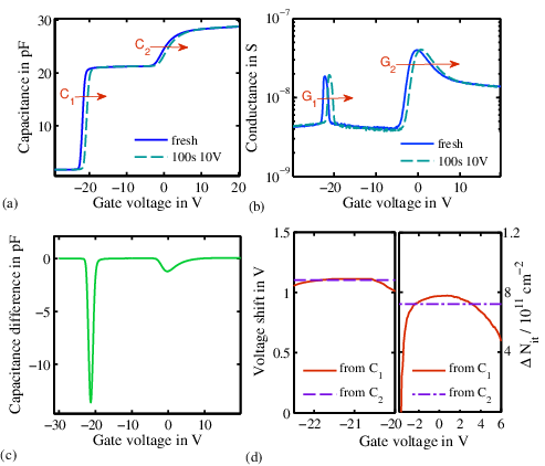
Figure 3.18: Capacitance (a) and conductance (b) characteristics before and after 100 s at 10 V. The difference between stressed and fresh curves determines the two regions where  can be calculated (c). The voltage shift (d) is calculated from the capacitance curve (solid
line) and from the position of the conductance peaks (dashed lines). The corresponding density of traps at the interface
can be calculated (c). The voltage shift (d) is calculated from the capacitance curve (solid
line) and from the position of the conductance peaks (dashed lines). The corresponding density of traps at the interface  is shown on the right axis (from [67]).
Even if the impedance characteristic cannot be directly analyzed to extract information about the trap states, we can compare the characteristics of a device before and after the application of stress, provided that the measurement parameters used are
constant. For example, in Fig. 3.18a and b the capacitance and conductance curve before and after a transient at 10 V for 100 s are shown. We note
that there are two regions where the two curves differ the most, that we call  and
and  for capacitance and
  and
and  for conductance. This is clarified in Fig. 3.18c, where the difference of the two curves is shown. We calculate the voltage shift in the following way: for every gate bias point of the stressed curve,
  , we have a capacitance
  . We find the same value in the fresh curve and interpolate the relative gate
bias
. We find the same value in the fresh curve and interpolate the relative gate
bias  . The difference between and gives the total voltage shift , which is reported in Fig. 3.18d, labeled “from ” and “from ”. We also calculate from the position of the conductance peak, by taking the difference of the gate biases
where the peak has its maximum. The result is shown in Fig. 3.18d, labeled “from ” and “from ”. The density of interface states is calculated with Eq. (1.1) and is estimated to be slightly less than 1012/cm2. We note that in the first region, around the threshold voltage, a
parallel shift occurs. Furthermore, the comparison of capacitance and conductance curves gives the same information. On the other hand, the from the capacitance curve in the second region, around the spill–over, shows a rising and
falling behavior. This is due to the slight distortion of the CV curve after stress. In fact, the rather high stress level of 10 V for 100 s can change the charge state of the interface and result in a different shape of the CV curve.
. The difference between and gives the total voltage shift , which is reported in Fig. 3.18d, labeled “from ” and “from ”. We also calculate from the position of the conductance peak, by taking the difference of the gate biases
where the peak has its maximum. The result is shown in Fig. 3.18d, labeled “from ” and “from ”. The density of interface states is calculated with Eq. (1.1) and is estimated to be slightly less than 1012/cm2. We note that in the first region, around the threshold voltage, a
parallel shift occurs. Furthermore, the comparison of capacitance and conductance curves gives the same information. On the other hand, the from the capacitance curve in the second region, around the spill–over, shows a rising and
falling behavior. This is due to the slight distortion of the CV curve after stress. In fact, the rather high stress level of 10 V for 100 s can change the charge state of the interface and result in a different shape of the CV curve.
First, we test this approach by comparing a fresh and a stressed device after a fake “stress” where only the AC bias is applied for 100 s. We investigate the impact of the measurement parameters by repeating this experiment with the same variations used in the previous paragraph. The results are shown in Fig. 3.19a: the extracted voltage shift is always zero, as expected. This means that the small–signal alone does not wear out the device. Furthermore, this proves that the device to device variation is small enough to be neglected.
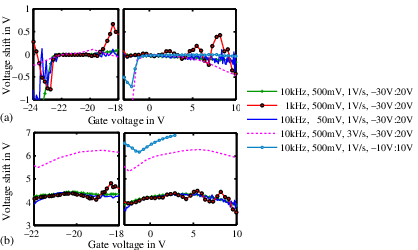
The second step consists in applying a real stress to the devices. Interestingly, in this case we find a strong dependence on some measurement parameters. Fig. 3.19b shows the after a stress of 100 s at 10 V. The result does not change when we vary the
small–signal parameters, like the frequency and the oscillator level. Using a sweep rate three times larger, or starting the sweep from −10 V instead of −30 V results in a variation of the extracted voltage shift of about 40%. We must conclude that the
measurement parameters impact not only the shape of the impedance characteristics of the device, but they can have a larger influence than a stress transient of 10 V applied for 100 s. This simple approach of evaluation therefore is not reliable since the measurement itself conceals the effect of the
stress. For this reason, we must develop a characterization method that enables us to evaluate the device degradation as accurately as possible. We present two such methodologies in the next section.
Previous: 3 Methodologies for electrical characterization of interface defects in GaN-based MIS-HEMTs Top: 3 Methodologies for electrical characterization of interface defects in GaN-based MIS-HEMTs Next: 3.3 Voltage shift methods