« PreviousUpNext »Contents
Previous: 4.3 Extraction of the activation energy and from experimental data Top: Home Next: 5.2 Results on devices with fluorinated interfaces
5 Electrical characterization of interface defects in GaN–based MIS–HEMTs
In this chapter we apply the experimental methods discussed in Chapter 3 and the physical model presented in Chapter 4 to our test structures. In the first place, we compare the MSM and the C–OTF experimental approaches and we discuss their outcomes on different samples. Then, we evaluate the impact of forward gate bias stress on device degradation due to the defects at the AlGaN/dielectric interface, and we extract the trap density. We use different GaN–based test structures: MIS and MIS–HEMTS with and without the barrier layer, with different bulk compositions and with different AlGaN surface chemical treatment. We characterize and compare them in order to understand the behavior of the interface traps and the impact of certain processes during production.
5.1 Results on devices with standard interface
In this first section we focus on structures with a standard AlGaN/dielectric interface. Such devices have been extensively investigated [47, 51] and they always display a linear dependence of the threshold voltage shift on the logarithm of time
under positive gate bias stress, from 100 ns to 10 ks. This implies a broad distribution of characteristic time constants of the interface traps, irrespective of variations of the Al content from 20% to 25%, of the thickness of the barrier (10 nm
to 25 nm), that of the dielectric (25 nm to 75 nm) and the dielectric material (SiN, SiO , AlO, HfO, HfSiO). As a preliminary step, we apply and compare the two
experimental methods introduced in Chapter 3.3. Then, we evaluate their response to positive gate bias stress and we calculate the density of traps present at the interface with the Primak approach, as described in Chapter 4.3.2.
, AlO, HfO, HfSiO). As a preliminary step, we apply and compare the two
experimental methods introduced in Chapter 3.3. Then, we evaluate their response to positive gate bias stress and we calculate the density of traps present at the interface with the Primak approach, as described in Chapter 4.3.2.
5.1.1 Comparison of experimental methods
We apply the MSM and the C–OTF methods on two different GaN/AlGaN MIS structures. The first has a 25 nm thick barrier and a UID GaN buffer; the second has a 50 nm thick AlGaN layer, its area is roughly four times larger and an additional silicon doped (1018/cm3) layer is inserted into the GaN, 100 nm from the interface with AlGaN.
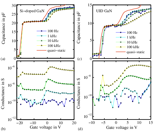
Figure 5.1: Impedance characteristics of the devices with the Si–doped layer: capacitance (a) and conductance (b) at various frequencies, and the same measurements on the structures with the UID GaN buffer (c and d). The quasi–static CV is also shown. All data has been measured with the impedance analyzer using the same parameters (from [67]).
Fig. 5.1 shows the impedance characteristics of the two test structures. In both cases we clearly observe a frequency dispersion, arising
from the dynamic response of the AlGaN barrier to the applied small–signal excitation, as discussed in detail in Section 3.2.1. The best estimate for the spill–over voltage is given by the quasi–static CV: the Si–doped sample has a  of −4 V, the UID structure of
−1 V.
of −4 V, the UID structure of
−1 V.
We apply a positive bias at the gate contact in order to bring the devices in spill–over conditions, and then we monitor the voltage drift. We use similar operating conditions for the two structures by choosing a voltage 9 V larger than [51]: the resulting stress voltage used in
this experiment is  5 V for the Si–doped and 8 V for the UID devices.
The MSM method is based on the comparison of the capacitance before and after stress. In particular, we measure in the proximity of the first steep capacitance step, where the sensitivity to  is very high. Unfortunately, the read–out voltage must be negative, thus bringing the
device into recovery conditions. The interval of time between the voltage switch and the measurement of the first experimental point causes a partial recovery from the applied stress. As a consequence, we systematically underestimate the real degradation by an
amount
is very high. Unfortunately, the read–out voltage must be negative, thus bringing the
device into recovery conditions. The interval of time between the voltage switch and the measurement of the first experimental point causes a partial recovery from the applied stress. As a consequence, we systematically underestimate the real degradation by an
amount  . In addition, at such gate bias buffer
defects may have an impact as well.
. In addition, at such gate bias buffer
defects may have an impact as well.
On the other hand, with the C–OTF method we make two approximations which result in a systematic overestimation of the voltage shift. First, we neglect the additional stress caused by the sweep when measuring the capacitance characteristic, and secondly,
we assume a parallel shift of the CV curve during stress. In addition, we miss a certain  because of the unavoidable
measurement delay.
because of the unavoidable
measurement delay.

The method which gives the most severe error depends on the relative time dependence of capture and emission processes. In fact, using the same time delay, depends on the amount of electrons
that can be emitted during this interval, while depends on the capture process at
the beginning of the stress transient. Recent studies on standard devices with UID GaN buffer have shown a similar temporal evolution of stress and recovery [52]. In this case, we would expect that the errors with the two methods are on the same order of
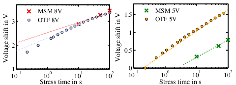
magnitude. In fact, the results in Fig. 5.2a confirm our hypothesis.
Interestingly, this is not the case for the Si–doped devices. As we can see from Fig. 5.2b, the MSM method severely underestimated
the in comparison to the C–OTF. The difference is about 40%. We explain this effect with the
presence of additional defects in the bulk, located in the Si–doped region, which become active when the negative read–out bias for the MSM technique is applied. In this way, the negative shift due to the buffer defects results in a strong underestimation of the
positive accumulated during stress.
In conclusion, the two methods give similar results for the structures with an UID GaN bulk. The C–OTF technique focuses on the stress transient, giving directly the temporal evolution of with a single measurement, while the MSM approach can be used for more complex
experiments of repetitive stress and recovery cycles. The presence of a highly doped layer inside the GaN buffer can result in a severe error when the MSM method is used, because buffer defects cause additional trapping phenomena at negative bias. On the
contrary, the data extracted with the C–OTF method is unaffected by those traps, and in this case is the most accurate characterization method.
5.1.2 Effect of forward gate bias stress
We further investigate the devices with the silicon–doped buffer using the C–OTF method. We focus on the dependence of the voltage shift on time, bias and temperature.
The results for different stress voltages at room temperature (30 °C) are summarized in Fig. 5.3. As expected, we observe a logarithmic behavior over time. We estimate the density of electrically active interface states at the interface to be on the order of 1013/cm2.
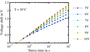

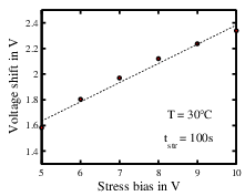
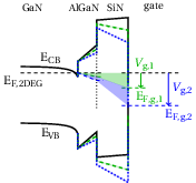

Figure 5.4: Dependence of the value on the gate bias (a) between 220 ms and 100 s at room temperature
(30 °C), from Fig. 5.3. The line is a guide to the eye. Schematic illustration of the AER concept (b). The band diagram is shown in
three situations: before stress (solid line), after stress at  (dashed) and after stress at
  (dotted).
Fig. 5.4a shows the bias dependence of the voltage shift between 220 ms and 100 s of stress. We see that an increase of gate
bias stress leads to a larger final device drift. This can be explained by considering the amount of trap states which are in a favorable position in energy to change their charge state as a function of  . When the external positive bias is applied
the band structure changes, lowering the conduction band edge. In this way, an additional number of defects are brought from above to below the Fermi level, thus acting as electron traps. This is sketched in Fig. 5.4b. The portion of accessible states is called the active energy region (AER) [27], and it increases with gate bias stress.
. When the external positive bias is applied
the band structure changes, lowering the conduction band edge. In this way, an additional number of defects are brought from above to below the Fermi level, thus acting as electron traps. This is sketched in Fig. 5.4b. The portion of accessible states is called the active energy region (AER) [27], and it increases with gate bias stress.
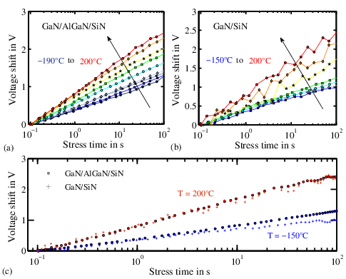
Figure 5.5: Isothermal forward gate bias stress experiments from cryogenic (−190 °C) to high (200 °C) temperature, for the GaN/AlGaN/SiN (a) and the GaN/SiN devices (b). Interestingly, the temporal behavior of the degra-
dation does not change much over a range of almost 400 °C. Comparison of the coldest and hottest stress experiment for the devices with and without an AlGaN layer (c): the similarity of the temporal evolution of implies the same qualitative degradation mechanism.
We investigate the influence of temperature by performing C–OTF experiments using a cryogenic probe station. In this way, we span a range of nearly 400 °C, from liquid nitrogen temperature (−190 °C) to the highest chuck
temperature (200 °C). We apply a stress bias of 5 V for 100 s. From the coldest to the hottest conditions we always observed a logarithmic behavior over time, as shown in Fig. 5.5a. The only difference with increasing temperature is an increase of the slope of .
We can compare the effect of positive stress on composite GaN/AlGaN MIS devices and similar structures that do not have an AlGaN layer. Obviously, the GaN/SiN samples do not have any 2DEG, but in this case the carriers are supplied by the Si–doped layer
buried in the GaN. For this reason they exhibit poor conductive properties, which explains the larger noise in the data with respect to the composite GaN/AlGaN measurements, as we can see in Fig. 5.5b. Nevertheless, we observe a qualitatively similar behavior to the previous case: increases linearly with the logarithm of time and higher temperatures lead to a faster
degradation. This result allows us to exclude that the transport through the barrier is the rate limiting effect. This is consistent with previous experiments which have investigated the role of the barrier in MIS–HEMT degradation. It has been shown that the barrier
becomes important for short stress times at low biases, while for long times and gate bias well above spill-over (like in our experiment) this is not the case [47]. Fig. 5.5c summarizes and makes a direct comparison of the two wafers with the standard interface at the coldest and highest temperature. Except for
the noise, the difference in absolute value of between the two cases is of about 10%.
5.1.3 Evaluation of the interface trap density
We apply the Primak method for the extraction of the density of interface traps,  , from the experimental data on the
GaN/AlGaN/SiN devices. The result is shown in Fig. 5.6.
, from the experimental data on the
GaN/AlGaN/SiN devices. The result is shown in Fig. 5.6.
The energy range accessible with our measurements is from 0.1 eV to 0.8 eV. The trap density spectra are distributed over the whole interval, never falling below 5 × 10¹²/(cm2 eV). The small increase of
to
2 × 10¹³/(cm2 eV) at low energies could be a hint to a normal distribution around a value below 0.1 eV. However, with our experimental setup we are sensitive only to this portion of the spectrum. Measurements at colder
temperatures or the evaluation of the device drift on shorter time scales would allow to extend the energy range to smaller values. The almost uniform distribution of activation energies from 0.2 eV to 0.8 eV gives rise to the observed uniformly
distributed time constants, which in turn cause the logarithmic behavior of the over time.
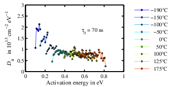
We can interpret this result as a clear indication of the disordered nature of the AlGaN/SiN interface. Physical–chemical investigations in fact suggest the presence of a non–stoichiometric interlayer, about 1 nm thick, where the density of point defects is very high. Although the origin of such defects is still under investigation, recent studies indicate the accumulation of oxygen impurities at the bottom of the SiN layer, which is in contact with the AlGaN [97].
The question whether these states are actually the surface donor states necessary for the 2DEG formation remains open. However, the comparison with the devices with the fluorinated AlGaN/SiN interface presented in the next Section leads to some interesting conclusions.
« PreviousUpNext »ContentsPrevious: 4.3 Extraction of the activation energy and from experimental data Top: Home Next: 5.2 Results on devices with fluorinated interfaces