2While the first transistor was developed in 1947 by using germanium as the semiconductor material and GaAs devices have demonstrated high switching speed, it is silicon which completely dominates the present semiconductor market. This development has arised due to the low cost of silicon CMOS technology. The fabrication processes and the device performance rely heavily on a number of natural properties of silicon, for instance, the availability of a good oxide. For alternative semiconductor materials much more expensive fabrication processes must be used, whereby the phenomenal yields achievable on a silicon CMOS line cannot be reached. One drawback of silicon is its relatively small carrier mobility. Since the device speed depends on how fast the carriers can be transported through the device channel under sustainable low operating voltages, silicon can be regarded as a relatively slow semiconductor. Today, it is commonly believed that a further improvement in the channel mobility beyond those that can be achieved with process-induced strain will be required in order to maintain continued commensurate device scaling. The higher carrier mobility offered by group-IV materials like SiGe compounds, germanium, and various heterostructures, for instance, biaxially strained silicon on relaxed SiGe, are required as new channel materials for bulk and on-insulator implementations [88,89,90].
While ion-implanted doping profiles are well studied in silicon for various dopant species and implantation conditions, such doping profiles are scarce in SiGe alloys as well as in pure Ge. An accurate and multi-dimensional simulation of ion implantation processes is required to optimize the doping profiles in these semiconductor materials for high-performance CMOS applications and optoelectronic devices. Since quantitatively predictive capabilities are a must for a Monte Carlo ion implantation simulator, the used models for implantations into silicon have been evaluated to extend the simulator to this wide class of materials on the basis of experimental results. For calibration purposes, a set of specifically selected experiments for arsenic and boron implantations into SiGe virtual substrates with different Ge content has been developed and carried out. Additional experimental results from other research groups obtained by arsenic and boron implantations into strained Si, relaxed SiGe layers with high Ge contents, and into Ge wafers have been included. The doping profiles in the investigated non-silicon materials are always compared to a reference doping profile in silicon, implanted under the same conditions. On the basis of these experiments various effects which influence the dopant distribution (e.g. Ge content in the alloy, damage accumulation, channeling effect) can be analyzed independently. The extended simulator is able to accurately predict the doping profiles in germanium and in SiGe alloys of arbitrary Ge content, and to estimate the produced point defects.
Silicon-germanium (SiGe) is a IV-IV compound semiconductor which offers enhanced carrier mobility and a higher dopant solubility compared to pure silicon. The remarkable potential of the SiGe material arises from the possibility to modify its properties by altering the composition. For instance, the band gap decreases from 1.12eV (pure silicon) to 0.66eV (pure germanium) at room temperature. The lattice parameter of the germanium crystal is 4.2% larger than that of silicon. Relaxed SiGe has a lattice parameter value which lies between those of the endpoint elements silicon and germanium depending on the Ge content in the alloy. Crystalline SiGe can be grouped into the two categories relaxed and strained. Strain engineering is used to enhance the carrier mobility for MOS transistors. By building different kinds of Si-SiGe heterostructures various properties for device design can be optimized. When silicon is epitaxially grown on SiGe, silicon forms a strained layer configuration up to a certain critical thickness. A strained SiGe layer can be grown on silicon in a similar way. A strained-Si/relaxed-SiGe structure produces tensile strain which primarily improves the electron mobility, while compressive strain obtained by a strained-SiGe/relaxed-Si structure boosts the hole mobility. Although the quality of SiGe virtual substrates or bulk wafers has steadily improved over the last years, the defect density is still too large to guarantee a reasonable yield in CMOS processing at present time [91].
While the ion moves through the simulation domain, a local crystal model (as
shown in Fig. 4.1) is built up around the actual ion position for
searching the next collision partner. The selection of the target atom species
for a collision event in Si
![]() Ge
Ge
![]() targets is
performed by probability
targets is
performed by probability ![]() for germanium and
for germanium and
![]() for silicon,
respectively. This random choice of the atom species in the crystalline model
is acceptable, because no ordering has been observed in bulk SiGe crystals
and ordering mechanisms in epitaxial grown SiGe layers are still under investigation.
for silicon,
respectively. This random choice of the atom species in the crystalline model
is acceptable, because no ordering has been observed in bulk SiGe crystals
and ordering mechanisms in epitaxial grown SiGe layers are still under investigation.
![\resizebox{1.0\linewidth}{!}{\rotatebox{0}{\includegraphics[clip]{figures/model_SiGe}}}](img443.png)
|
|
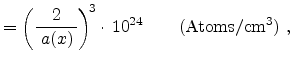
Table 4.1 summarizes some important physical properties relevant for
ion implantation in silicon, germanium, and Si
![]() Ge
Ge
![]() alloys with
alloys with
![]() ,
,
![]() , and
, and
![]() . A linear interpolation
between the endpoint elements silicon and germanium is used to derive the values
for the average atomic mass and the Debye temperature in SiGe for different
compositions. The values of the SiGe lattice parameter were calculated by using
the quadratic approximation (4.1). The lattice parameter at a Ge
concentration
. A linear interpolation
between the endpoint elements silicon and germanium is used to derive the values
for the average atomic mass and the Debye temperature in SiGe for different
compositions. The values of the SiGe lattice parameter were calculated by using
the quadratic approximation (4.1). The lattice parameter at a Ge
concentration ![]() ,
, ![]() , determines the atomic density
, determines the atomic density ![]() for
Si
for
Si
![]() Ge
Ge
![]() according to (4.2).
Finally, the Si
according to (4.2).
Finally, the Si
![]() Ge
Ge
![]() material density
material density ![]() is
obtained by inserting equation (4.2) into equation (4.3) and
by proportionately averaging over the atomic weights of silicon and germanium,
is
obtained by inserting equation (4.2) into equation (4.3) and
by proportionately averaging over the atomic weights of silicon and germanium,
![]() and
and ![]() .
.
For the simulation with MCIMPL-II the properties of an arbitrary SiGe material
segment can be uniquely defined in the input WSS file by specifying the three
quantities molecular formula (composition), material density,
and crystal orientation.
The electronic stopping process is calculated with the empirical Hobler model.
The only physical parameter required for this model is the impact parameter
which is determined when selecting a collision partner. Due to the fact that the
model implies a dependence on the charge and the mass of the atoms of the target
material, the electronic stopping power is averaged in the case of a compound
material like SiGe. The electronic stopping power of SiGe is larger compared
with silicon, which is caused by the higher electron density due to the
electron-rich germanium atom [98].
The calibration of the model for Si
![]() Ge
Ge
![]() targets
was performed by arranging the Lindhard correction parameter
targets
was performed by arranging the Lindhard correction parameter ![]() as a
linearly rising function of the germanium fraction
as a
linearly rising function of the germanium fraction ![]() . For the other three
parameters of the model the values from crystalline silicon could be applied.
We found the relations (4.6) and (4.7) by comparing simulated profiles
with SIMS profiles, which determine the parameters
. For the other three
parameters of the model the values from crystalline silicon could be applied.
We found the relations (4.6) and (4.7) by comparing simulated profiles
with SIMS profiles, which determine the parameters ![]() for arsenic and
for arsenic and
![]() for boron.
for boron.
![\resizebox{1.0\linewidth}{!}{\rotatebox{0}{\includegraphics[clip]{figures/As_SiGe_60.eps}}}](img484.png)
|
![\resizebox{1.0\linewidth}{!}{\rotatebox{0}{\includegraphics[clip]{figures/As_SiGe35.eps}}}](img485.png)
|
![\resizebox{1.0\linewidth}{!}{\rotatebox{0}{\includegraphics[clip]{figures/B_SiGe53_20.eps}}}](img486.png)
|
![\resizebox{1.0\linewidth}{!}{\rotatebox{0}{\includegraphics[clip]{figures/B_SiGe_5.eps}}}](img488.png)
|
![\resizebox{0.98\linewidth}{!}{\rotatebox{0}{\includegraphics[clip]{figures/hetero-comb}}}](img490.png)
|
Fig. 4.6 shows the strained-Si/relaxed-SiGe heterostructure which is used to investigate the impact of strain on ion implantation. Relaxed SiGe layers are epitaxially grown on (100) silicon substrates using a grading technique to obtain the desired Ge composition. Next a constant composition layer is grown to spatially separate the subsequently grown strained silicon layer from the misfit dislocations contained in the graded SiGe layer. When silicon is grown on SiGe, the lattice mismatch between the two materials can be accommodated by uniform lattice strain in sufficiently thin silicon layers [102]. If silicon is grown beyond its critical thickness, the strained crystal relaxes to its natural size and a high concentration of dislocations is introduced. Fig. 4.6 shows also typical experimetal data for the critical layer thickness which depends on growth rates, growth temperature, SiGe surface orientation, and mostly on the Ge concentration [96].
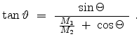
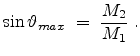
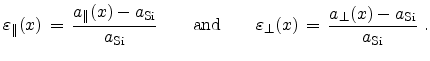
![$\displaystyle a_{\perp}(x) = a_{\mathrm{Si}} \left[1 - \frac{2 C_{12}}{C_{11}}\...
...arallel}(x)}{a_{\mathrm{Si}}} - 1 \right)\right]\quad(\mathrm{\mathring A)} ,$](img495.png) |
(4.9) |
The constraints for the two lattice parameters in strained silicon are given by
| (4.10) |
Fig. 4.8 shows that the simulated boron profiles in strained and
unstrained silicon are almost identically distributed, and the simulation
result agrees well with the SIMS data. It is not possible to characterize
arsenic concentration profiles in Si
![]() Ge
Ge
![]() by SIMS
analysis with a resolution larger than about three orders-of-magnitude due to
similar atomic masses of arsenic and germanium [99].
As shown in Fig. 4.9 the Monte Carlo simulation can help to get a realistic
continuation of the doping profile below the arsenic detection limit.
The discrepancy between the predicted and measured doping profiles near the
wafer surface may arise from a measurement error in this region. Feedback from
industry revealed that this error can be eliminated by the deposition of
amorphous silicon on the wafer before the SIMS measurement. Using this
procedure, SIMS profiles show an increase in the near-surface region too.
However, the simulation results in Fig. 4.9 demonstrate that the
arsenic distribution in strained silicon has a slightly deeper penetration
compared to unstrained silicon, which can be explained by a stress-induced
volume dilation of the material. Strained silicon on Si
by SIMS
analysis with a resolution larger than about three orders-of-magnitude due to
similar atomic masses of arsenic and germanium [99].
As shown in Fig. 4.9 the Monte Carlo simulation can help to get a realistic
continuation of the doping profile below the arsenic detection limit.
The discrepancy between the predicted and measured doping profiles near the
wafer surface may arise from a measurement error in this region. Feedback from
industry revealed that this error can be eliminated by the deposition of
amorphous silicon on the wafer before the SIMS measurement. Using this
procedure, SIMS profiles show an increase in the near-surface region too.
However, the simulation results in Fig. 4.9 demonstrate that the
arsenic distribution in strained silicon has a slightly deeper penetration
compared to unstrained silicon, which can be explained by a stress-induced
volume dilation of the material. Strained silicon on Si![]() Ge
Ge![]() has
a strain
has
a strain
![]() and
approximately 99% of the atomic density of unstrained silicon.
and
approximately 99% of the atomic density of unstrained silicon.
![\resizebox{0.815\linewidth}{!}{\rotatebox{0}{\includegraphics[clip]{figures/B_SSi}}}](img505.png)
|
In recent years, deep-submicron germanium MOS transistors have been processed
in a silicon-like process flow by using either germanium oxynitride
(GeO
![]() N
N
![]() ) [105] or Hafnium oxide (HfO
) [105] or Hafnium oxide (HfO![]() )
based high-k dielectrics [106,107] as the gate insulator.
The diffusion of the p-type dopant boron is suppressed while the diffusion
of the n-type dopants phosphorus, arsenic, and antimony is increased in
SiGe and germanium compared with silicon [108]. Thus, the formation
of ultra-shallow junctions in germanium is facilitated for p-MOS transistors,
while it becomes more challenging for n-MOS devices.
It was found in [107] that the junction leakage is about four
decades higher for germanium at a chip temperature of 110
)
based high-k dielectrics [106,107] as the gate insulator.
The diffusion of the p-type dopant boron is suppressed while the diffusion
of the n-type dopants phosphorus, arsenic, and antimony is increased in
SiGe and germanium compared with silicon [108]. Thus, the formation
of ultra-shallow junctions in germanium is facilitated for p-MOS transistors,
while it becomes more challenging for n-MOS devices.
It was found in [107] that the junction leakage is about four
decades higher for germanium at a chip temperature of 110![]() C compared
with silicon. The reduction of the relatively large leakage current will be
a key issue for Ge-CMOS technology to obtain devices with reasonably low
C compared
with silicon. The reduction of the relatively large leakage current will be
a key issue for Ge-CMOS technology to obtain devices with reasonably low
![]() current. It is reported in [105], that the leakage
current of boron implanted p
current. It is reported in [105], that the leakage
current of boron implanted p
![]() /n junctions in germanium can be
reduced down to the order of
/n junctions in germanium can be
reduced down to the order of ![]() A/cm
A/cm![]() with annealing at
400
with annealing at
400![]() C, which is considered acceptable for device operation.
Ge-rich Si
C, which is considered acceptable for device operation.
Ge-rich Si
![]() Ge
Ge
![]() alloys
alloys
![]() and germanium have been recognized as promising materials for photodetectors
in fibre-optical transmission systems due to the high optical absorption
coefficient for an operation at a wavelength of 1.3
and germanium have been recognized as promising materials for photodetectors
in fibre-optical transmission systems due to the high optical absorption
coefficient for an operation at a wavelength of 1.3![]() m in the near
infrared (NIR) regime [109,110]. The use of epitaxial Ge-on-Si
technology allows the integration of germanium pin-photodiodes with CMOS
circuits on a silicon chip to build optical communication receivers with
low fabrication costs. Optical chip-to-chip communication solutions and
even optical on-chip interconnects will be required to meet the challenges
of differentiated, high-performance systems in the future.
m in the near
infrared (NIR) regime [109,110]. The use of epitaxial Ge-on-Si
technology allows the integration of germanium pin-photodiodes with CMOS
circuits on a silicon chip to build optical communication receivers with
low fabrication costs. Optical chip-to-chip communication solutions and
even optical on-chip interconnects will be required to meet the challenges
of differentiated, high-performance systems in the future.
|
Ion implantation is a crucial step for processing these device structures. An experimental and simulation study for introducing boron ions into (100) germanium wafers in the energy range from 5 to 40keV is presented in this section [112]. The successful calibration of the simulator MCIMPL-II for germanium is demonstrated by comparing the predicted boron profiles with SIMS data. A doping profile in germanium is shallower than in silicon for any given energy due to the larger nuclear and electronic stopping power. We found also that the produced crystal damage is significantly reduced in germanium, which is consistent with former experimental observations [113] indicating that boron-implanted germanium remains essentially crystalline.
![\resizebox{1.0\linewidth}{!}{\rotatebox{0}{\includegraphics[clip]{figures/kp.eps}}}](img515.png)
|
An advantage of the Monte Carlo simulation is that the used Kinchin-Pease model
(as described in Section 3.1.4) allows to estimate the produced vacancies in the
germanium crystal. Note that equal local concentrations of vacancies and interstitials
are assumed, since the recoils themselves are not individually followed in our
computationally fast simulation approach. However, a critical model parameter is
the threshold displacement energy required for the ion to displace a target atom.
A displacement energy ![]() of 15eV has become widely accepted for silicon.
We fitted a value of
of 15eV has become widely accepted for silicon.
We fitted a value of
![]() 30eV for germanium by comparison of simulated
boron profiles with SIMS measurements.
Fig. 4.10 shows the number of produced point defects for a damage cascade,
calculated with the modified Kinchin-Pease model. The used value for the
displacement energy in germanium is in good agreement with
30eV for germanium by comparison of simulated
boron profiles with SIMS measurements.
Fig. 4.10 shows the number of produced point defects for a damage cascade,
calculated with the modified Kinchin-Pease model. The used value for the
displacement energy in germanium is in good agreement with
![]() eV
which was deduced by Mitchell in 1957 for germanium [114].
The larger
eV
which was deduced by Mitchell in 1957 for germanium [114].
The larger ![]() value is responsible for the generation of significantly fewer
point defects by a boron ion in germanium compared with silicon for any amount of
transferred energy
value is responsible for the generation of significantly fewer
point defects by a boron ion in germanium compared with silicon for any amount of
transferred energy ![]() to the primary knock-on atom of a cascade.
The reduced damage production by ion implantation in crystalline germanium is
consistent with former experimental observations [113].
to the primary knock-on atom of a cascade.
The reduced damage production by ion implantation in crystalline germanium is
consistent with former experimental observations [113].
![\resizebox{1.0\linewidth}{!}{\rotatebox{0}{\includegraphics[clip]{figures/traj.eps}}}](img518.png)
|
The Lindhard correction parameter ![]() of the empirical electronic stopping
model, which is explained in Section 3.1.3, has been calibrated to adjust the
strength of the electronic stopping power for boron ions in germanium.
We increased the empirical parameter value from
of the empirical electronic stopping
model, which is explained in Section 3.1.3, has been calibrated to adjust the
strength of the electronic stopping power for boron ions in germanium.
We increased the empirical parameter value from
![]() for silicon
to a value of 1.9 for germanium.
for silicon
to a value of 1.9 for germanium.
In the following simulation study, at least ![]() trajectories were calculated
for a one-dimensional boron profile. Fig. 4.11 shows the visualization
of ten arbitrarily selected boron trajectories in silicon and in germanium.
This comparison demonstrates that the larger nuclear and electronic stopping
power of germanium, in particular the stronger backscattering of boron ions in
germanium, typically reduces the trajectory length.
trajectories were calculated
for a one-dimensional boron profile. Fig. 4.11 shows the visualization
of ten arbitrarily selected boron trajectories in silicon and in germanium.
This comparison demonstrates that the larger nuclear and electronic stopping
power of germanium, in particular the stronger backscattering of boron ions in
germanium, typically reduces the trajectory length.
Fig. 4.15 compares the simulated vacancy concentration profiles in silicon
and in germanium associated with the 20keV boron implantations shown in
Fig. 4.14. The vacancy maximum is not at the wafer surface, since the
electronic stopping process dominates at high initial energies of the ions, when
they enter the crystal. A boron ion enters most likely a channel at the surface
and despite of the tilted incident direction it can stay at least a short distance
inside a channel.
The higher displacement energy of 30eV, the stronger backscattering of boron ions
in germanium, and the smaller energy transfer ![]() from the ion to the
primary recoil of a cascade are mainly responsible for the significantly smaller
damage production in germanium. Privious experimental boron implantation results
in germanium [113] performed up to a dose of
from the ion to the
primary recoil of a cascade are mainly responsible for the significantly smaller
damage production in germanium. Privious experimental boron implantation results
in germanium [113] performed up to a dose of
![]() within the energy range of 25-150keV revealed that 100% of the boron ions are
immediately active after implantation without thermal annealing since
boron-implanted germanium remains crystalline.
This is a unique phenomenon, since an annealing step is required for every other
dopant species implanted in silicon or germanium in order to activate a significant
amount of dopants. Finally, Fig. 4.16 illustrates the dose dependence of
40keV boron profiles in germanium, which were simulated with the Kinchin-Pease
model. It is obvious that the shape of the profiles is influenced by the damage
accumulation in the crystal.
within the energy range of 25-150keV revealed that 100% of the boron ions are
immediately active after implantation without thermal annealing since
boron-implanted germanium remains crystalline.
This is a unique phenomenon, since an annealing step is required for every other
dopant species implanted in silicon or germanium in order to activate a significant
amount of dopants. Finally, Fig. 4.16 illustrates the dose dependence of
40keV boron profiles in germanium, which were simulated with the Kinchin-Pease
model. It is obvious that the shape of the profiles is influenced by the damage
accumulation in the crystal.
|
![\resizebox{1.0\linewidth}{!}{\rotatebox{0}{\includegraphics[clip]{figures/B_Ge_20.eps}}}](img527.png)
|
![\resizebox{1.0\linewidth}{!}{\rotatebox{0}{\includegraphics[clip]{figures/B_Ge_5.eps}}}](img528.png)
|
![\resizebox{1.0\linewidth}{!}{\rotatebox{0}{\includegraphics[clip]{figures/B_cmpSiGe.eps}}}](img529.png)
|
![\resizebox{1.0\linewidth}{!}{\rotatebox{0}{\includegraphics[clip]{figures/Vac_SiGe.eps}}}](img530.png)
|
The simulated point responses in crystalline silicon and germanium are shown in
Fig. 4.17 and Fig. 4.18 to study quantitatively the lateral and
vertical penetration of boron ions. The used two-and-a-half dimensional input
geometry has a depth dimension of 40nm, and the slot width of the implantation
window in an impenetrable mask is 8nm. A high-resolution mesh which consists of
33181 grid points and 144159 tetrahedrons is added to the input structure to
resolve the implanted boron distribution. Boron is implanted with an energy of
10keV, a dose of
![]() , and the ion beam is 7
, and the ion beam is 7![]() tilted in such a way that the lateral component of the incident direction is
parallel to the direction of view (
tilted in such a way that the lateral component of the incident direction is
parallel to the direction of view (![]() direction). Therefore, the
presented point responses are symmetric. Approximately 420000 simulated boron
ions of a total number of 50 million ions can enter the substrate at the mask
opening and contribute to the Monte Carlo result represented by the internal
histogram cells.
direction). Therefore, the
presented point responses are symmetric. Approximately 420000 simulated boron
ions of a total number of 50 million ions can enter the substrate at the mask
opening and contribute to the Monte Carlo result represented by the internal
histogram cells.
The visualization of single trajectories in silicon and in germanium (as
shown in Fig. 4.11) and in particular the comparison of the point
responses indicate that the boron distribution in germanium is significantly
reduced in the vertical direction, while the lateral profile is quite similar
in silicon and germanium. Additionally, it can be observed that the channeling
tail is closely centered around the
![]() axis in both cases.
This demonstrates that in (100) silicon and in (100) germanium, axial
channeling in the
axis in both cases.
This demonstrates that in (100) silicon and in (100) germanium, axial
channeling in the
![]() direction dominates by far over channeling
in other directions.
direction dominates by far over channeling
in other directions.
As demonstrated in this study, the used physics-based simulation approach in combination with experimental results allows to get a comprehensive understanding of implantation-related phenomenons in germanium.
![\resizebox{0.86\linewidth}{!}{\rotatebox{0}{\includegraphics[clip]{figures/pointSi.eps}}}](img535.png)
|
![\resizebox{0.86\linewidth}{!}{\rotatebox{0}{\includegraphics[clip]{figures/pointGe.eps}}}](img536.png)
|
![\resizebox{1.0\linewidth}{!}{\rotatebox{0}{\includegraphics[clip]{figures/model_SSi-sw.eps}}}](img491.png)
![\resizebox{0.815\linewidth}{!}{\rotatebox{0}{\includegraphics[clip]{figures/As_SSi}}}](img506.png)
![\resizebox{1.0\linewidth}{!}{\rotatebox{0}{\includegraphics[clip]{figures/B_Ge_40.eps}}}](img534.png)