|
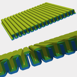
A simulation for a moving boundary using the Level Set method has been developed at this institute. The simulator uses Level Sets in order to identify and advance silicon wafer surfaces and interfaces between different chemicals on a silicon chip for various physical processes. A one-dimensional thermal oxidation model has been implemented in this environment, allowing for the simultaneous advancement of multiple surfaces. The interface between the oxide and ambient moves with a positive velocity towards the ambient, while the interface between the oxide and silicon moves with a negative velocity towards the silicon. The implemented simulator uses the linear and parabolic rate constants, as defined by the Deal-Grove and Massoud models, which are well suited for thick and thin oxide growths, respectively.
Modern lithographic methods are reaching the edge of their potential and nano-lithography using Atomic Force Microscopy (AFM) is a promising alternative for the manufacture of nanometer sized devices. The ability to grow oxides at nanometer precision is essential for modern processes. Models for the local anodic oxidation of silicon using Scanning Tunnelling Microscopy (STM) and AFM have been developed and implemented in the Level Set process simulator, using Monte Carlo methods. The implementation of further processing steps is easily incorporated within this environment. An empirical model for the width and height of an oxide nanowire using AFM has also been developed and implemented within the simulator. The height and width of an oxide pattern depend on the applied bias voltage, pulse time, humidity, and wafer orientation. An empirical model is used to generate the height and width of the oxide pattern, followed by a Monte Carlo implementation. Particles are generated using a random Lorentzian or Gaussian distribution and accelerated to the silicon surface. Upon contact with the surface, each particle forces an oxide to grow at the impact location, partially towards the ambient and partially towards the silicon wafer. The resulting oxide pattern has the height and width measured in published experiments and deduced in the developed empirical models.
Upon further investigation, treating the AFM needle tip as a static negative charge, it was determined that an electric field is generated towards the silicon surface. This causes an induced charge density on the silicon surface. Using the generated electric charge density and a Monte Carlo simulator, it has been shown that the Lorentzian profile is better suited to represent the final pattern of the oxide dot when compared with the Gaussian profile This has been confirmed by a thin lateral oxide growth shown in the Lorentzian profile.
|