|
Elevated ambient temperatures and high operating gate voltages alter the device parameters (e.g. Vth, gm, ...) of Metal-Oxide-Semiconductor Field-Effect Transistors (MOSFET).
This phenomenon is known as the Negative Bias Temperature Instability (NBTI) and limits the operating lifetime of the transistor.
NBTI belongs to the most important reliability issues in the semiconductor industry nowadays and is studied massively in terms of its physical behavior.
The latest promising attempt to model the NBTI phenomenon is based on Non Radiative Multiphonon (NMP) theory.
It assumes the conservation of the total energies of existing defects in the oxide of the transistor and has already reproduced measurement
data of small area devices containing only few defects.
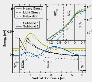
In order to reduce NBTI, buried SiGe channel p-MOSFETs with a thick SiGe quantum well of a high Ge-fraction (55%) and a thin SiCap were introduced. These devices are subjected to NBTI-stress using various stress voltages and temperatures. The measurement results can then be checked against the simulation. Therefore the previously mentioned model was refined by incorporating quantum mechanical effects as follows: To obtain the wavefunctions of the subbands in the channel of the MOSFET, the Schrödinger and Poisson equation were solved self-consistently using the Vienna Schrödinger-Poisson solver (VSP2), on the results shown in the Figure 1. The carrier concentration is calculated by treating the quasi-bound states as a two-dimensional electron gas with Fermi-Dirac distribution and the continuum states as 3D electron gas.
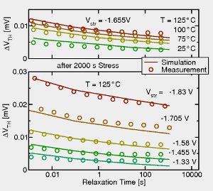
To describe NBTI on a macroscopic scale, the configurational energies for a large number of defects are assumed to be normally distributed and the depth into the oxide is varied. For each subband the obtained transition rates between the substrate and the defects determine the occupancy of the individual defects at certain stress or relaxation times. These defect occupancies then have to be summed up over all subbands in order to finally determine the visible degradation. The relaxation sequence after more than 2000s of stress is compared to experimental data at different temperatures and for different stress voltages, as shown in the Figure 2. Despite device to device-deviations, as various MOSFETs have to be used for the measurements to avoid pre-stress, it can be clearly seen that the measurements are very well reproduced using the new model.
|