|
High Electron Mobility Transistors GaN-based (HEMTs) are considered for high-power, high-frequency applications in a wide temperature range. Reliable software tools for DC and AC simulations of the devices are required for the further development and optimization of the devices. Depending on the device dimensions, a new drift-diffusion transport model or hydrodynamic approach are employed. Appropriate material models, which account for the peculiarities of the material systems, are developed and calibrated against experimental data and results from our own Monte Carlo simulations. We focus on GaN, AlN, InN, and their respective alloys.
We focus on different structures such as single or double heterojunction AlGaN/GaN HEMTs, as well as novel InAlN/GaN transistors. Our work also includes optimization for various applications (high-power, high-frequency or high-breakdown), involving different enhancement techniques. We account for all relevant physical effects. Our sets of material and model parameters are validated against experimental data in a wide temperature range. Studies of the device performance at elevated temperatures are performed.
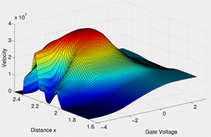
Since device transconductance is detrimental to intermodulation distortion, we focus on transconductance collapse at higher gate-voltages specific to HEMT structures. We explore the electric field distribution as well as the corresponding carrier velocity. Optimization techniques for the source-gate region are studied.
A further research topic is the simulation of novel solar cells. This includes new materials for back surface passivation for sub 300μm thick Silicon cells, as well as multi-junction structures based on Ge, GaAs, and InGaN.
|