|
Hot-Carrier Degradation (HCD) is rather complicated to model because it includes three different but strongly connected aspects. In fact, carriers interacting with the silicon/silicon dioxide interface break Si-H bonds, thereby generating traps at or near this interface and thus the microscopic mechanisms for defect creation have to be properly described. The information on how efficiently these carriers trigger the bond dissociation process is provided by a thorough carrier transport treatment. Furthermore, these generated traps can capture carriers and thus distort the electrostatics of the transistor and degrade carrier mobility.
We use a physics-based HCD model, which includes three main modules: a carrier transport module, a module for modeling of microscopic mechanisms of defect creation and a module for the simulation of the characteristics of the degraded devices. The carrier transport module calculates a set of carrier energy distribution functions at any position in the Metal-Oxide-Semiconductor Field-Effect Transistor (MOSFET) for a particular device architecture and stress/operating conditions. For this purpose we employ the full-band Monte-Carlo device simulator MONJU. Then the information about the carrier distribution is used to generate interface state density profiles. These profiles are then loaded to a circuit and device simulator MINIMOS-NT, which calculates the characteristics of the degraded device.
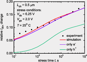
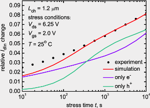
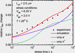
Recent results conclude that it is not sufficient to consider only channel electrons. Since secondary holes are generated by impact ionization and then accelerated by the electric field towards the source, thereby creating interface states shifted with respect to the electron-induced ones. As a result, the interface state fraction induced by holes is much less than their relative contribution to the linear drain current change. The model was calibrated in a manner to represent the linear drain degradation observed in 5V n-MOSFETs with various channel lengths (0.5, 1.2, and 2.0μm) for all the devices with the same set of fitting parameters and reveals a good agreement between experimental and theoretical results.
|