4.2 Elastic Tunneling
Tewksbury[23] assumed elastic tunneling of electrons and holes into and out of oxide
defects as the mechanism responsible for charge trapping. The use of his model
has been suggested by Huard et al. [58] in order to explain the recoverable
part of the NBTI degradation. In this section, Tewksbury’s model will be
reviewed, extended for an application of present-day devices with small gate
thicknesses, and referred to as the elastic tunneling model (ETM) in the
following.
The approach applied in this thesis relies on rate equations for tunneling into one
trap. The required rate expressions  and
and  are given by the equations
(2.45) and (2.46), which already incorporate all elastic tunneling transitions between
one trap and the numerous band states. Due to their analytical complexity, these rate
equations are solved numerically using the numerical iteration scheme presented in
Section 3.2. The used simple first-order partial differential equation reads
are given by the equations
(2.45) and (2.46), which already incorporate all elastic tunneling transitions between
one trap and the numerous band states. Due to their analytical complexity, these rate
equations are solved numerically using the numerical iteration scheme presented in
Section 3.2. The used simple first-order partial differential equation reads
with the electron and hole trapping times approximated as The electron ( ) and hole (
 ) occupancy are defined as with
  being the Fermi-Dirac distribution. The above rate equation features the
same structure as that of equation (4.1). Therefore, the same mathematical
implications as for the phenomenological model hold true for the ETM.
Furthermore, equation (4.6) covers all four basic transitions illustrated Fig. 4.2 so
that it can be viewed as a comprehensive description of elastic tunneling in
MOSFETs.
being the Fermi-Dirac distribution. The above rate equation features the
same structure as that of equation (4.1). Therefore, the same mathematical
implications as for the phenomenological model hold true for the ETM.
Furthermore, equation (4.6) covers all four basic transitions illustrated Fig. 4.2 so
that it can be viewed as a comprehensive description of elastic tunneling in
MOSFETs.
4.2.1 The Behavior of A Single Trap
In this chapter, the investigations are focused on NBTI in pMOSFETs since these
devices attract a large industrial interest at the moment. Therefore, only hole
tunneling from the substrate valence band will be addressed in the following.
Naturally, the basic statements will also remain valid for electron tunneling in the
case of PBTI in nMOSFETs and for the different dielectric materials used in modern
device technologies. For the trapping dynamics,  and
and  in
in
 and
and  of equation (4.6) are the most sensitive factors.
These quantities determine the basic properties of the ETM and will be discussed in
detail in this section.
of equation (4.6) are the most sensitive factors.
These quantities determine the basic properties of the ETM and will be discussed in
detail in this section.
The trapping dynamics are described by the rate equation (4.6), which has
the same forward  and reverse
  rate considering hole trapping
(
rate considering hole trapping
( ).
This special form implies that the occupancy of the trap
).
This special form implies that the occupancy of the trap  equilibrates to that of
the valence band states at the same energy
equilibrates to that of
the valence band states at the same energy  . For steady state conditions,
  reads
reads
where  and
and  take the role of
  and
and  in (4.2), respectively. The
above equation shows that the trap occupancy is eventually governed by the
relative magnitude of
in (4.2), respectively. The
above equation shows that the trap occupancy is eventually governed by the
relative magnitude of  and
and  . Both time constants are most
strongly affected by the exponential decay of the Fermi-Dirac distribution. This
dependence is pointed out in Fig. 4.3, where the hole capture and emission
times are plotted with respect to the trap energy
. Both time constants are most
strongly affected by the exponential decay of the Fermi-Dirac distribution. This
dependence is pointed out in Fig. 4.3, where the hole capture and emission
times are plotted with respect to the trap energy  . In the region below
 , the hole occupancy
  decreases by several orders of magnitude per
 so that the hole capture times
  by far exceed the corresponding
emission times
by far exceed the corresponding
emission times  . Therefore, no effective hole trapping can take place in
this region, irrespectively of the temperature. By contrast above
. Therefore, no effective hole trapping can take place in
this region, irrespectively of the temperature. By contrast above  , the
exponential decay of
, the
exponential decay of  causes an increase in the hole emission times
  ,
which gives rise to hole trapping there. That is,
,
which gives rise to hole trapping there. That is,  can be regarded as a
demarcation energy between both regions. This fact is also reflected in the
equilibrium solution (4.12) when using the definitions of
can be regarded as a
demarcation energy between both regions. This fact is also reflected in the
equilibrium solution (4.12) when using the definitions of  and
and  .
.
As a consequence, the trap occupancy is governed by the position of the substrate Fermi level
in equilibrium.
As mentioned before, the most sensitive factors in the tunneling rates of equation
(4.6) are the Fermi-Dirac distribution and the WKB factor. In contrast to  and
and
 , the latter is a function of
  and cannot be taken out of the integrals in the
rate expressions (2.45) and (2.46). As shown in Fig. 4.4,
and cannot be taken out of the integrals in the
rate expressions (2.45) and (2.46). As shown in Fig. 4.4,  and
and
 , the matrix element without the WKB factor, are subject
to small variations so that they weakly affect the tunneling rates. Since
the WKB factor falls off quickly with increasing
, the matrix element without the WKB factor, are subject
to small variations so that they weakly affect the tunneling rates. Since
the WKB factor falls off quickly with increasing  , the integral (2.46)
delivers the largest contribution close to the trap level
, the integral (2.46)
delivers the largest contribution close to the trap level  . Therefore, it
makes sense to approximate the rate integral (2.46) by dividing it through
. Therefore, it
makes sense to approximate the rate integral (2.46) by dividing it through
 and define the resulting expression as
  . This new
quantity incorporates the weak dependences on
. This new
quantity incorporates the weak dependences on  while the sensitive factors,
namely
while the sensitive factors,
namely  or
or  and the WKB factor, are separated. Due to the small variations
of
and the WKB factor, are separated. Due to the small variations
of 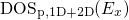 and
and 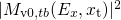 ,
,  shows small changes with
 compared to
  and
and 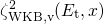 (see Fig. 4.5). This fact justifies
approximations[23, 160, 106, 105], in which
(see Fig. 4.5). This fact justifies
approximations[23, 160, 106, 105], in which  as a prefactor of the WKB
factor is approximated as a constant. Using the above definitions, the rate equation
for holes reads:
as a prefactor of the WKB
factor is approximated as a constant. Using the above definitions, the rate equation
for holes reads:

For the time evolution of charge trapping, 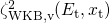 becomes the essential
factor (cf. Fig. 4.6). It shows an exponential decay with increasing trap depth, which
results in a shift of
becomes the essential
factor (cf. Fig. 4.6). It shows an exponential decay with increasing trap depth, which
results in a shift of  and
and  towards larger times (cf. Fig. 4.7). Note that the
energy of the tunneling charge carrier also impacts the WKB factor and the capture
and the emission times. Since the energy dependence of the WKB factor enters
both the capture and the emission times, their relative magnitude remains
unaffected and the above argumentation of
towards larger times (cf. Fig. 4.7). Note that the
energy of the tunneling charge carrier also impacts the WKB factor and the capture
and the emission times. Since the energy dependence of the WKB factor enters
both the capture and the emission times, their relative magnitude remains
unaffected and the above argumentation of  as a demarcation energy remains
valid.
as a demarcation energy remains
valid.
In conclusion, the following findings have been made: The equilibrium charge state of
an oxide defect is directly determined by the Fermi level in the substrate. When  is situated above
  , the defect will capture a hole if the defect is initially occupied
by an electron. Vice versa, positively charged defects with
, the defect will capture a hole if the defect is initially occupied
by an electron. Vice versa, positively charged defects with  below
below  will
emit their holes. However, this relationship does not make any statement
about the time point when the tunneling transitions occur. This is solely
given by the respective capture (
will
emit their holes. However, this relationship does not make any statement
about the time point when the tunneling transitions occur. This is solely
given by the respective capture ( ) or emission (
 ) time constant.
The actual trapping times are given by the WKB factor, which predicts
increasing capture (
) time constant.
The actual trapping times are given by the WKB factor, which predicts
increasing capture ( ) and emission (
 ) times for larger tunneling
distances.
) times for larger tunneling
distances.
4.2.2 Spatially and Energetically Distributed Traps
In the previous sections, only the behavior of single traps has been addressed but
NBTI is actually caused by charging or discharging of a multitude of defects. This
means that the degradation has to be understood as a superposition of several
trapping events. It must be considered that the individual defects differ in their
properties, such as their spatial depth and their energetical position within the oxide
bandgap. The defects in this model are assumed to be bulk traps, which are
scattered across the whole dielectric. The distribution in the trap levels
can be attributed to variations in bond length and angles, which impact
the energy levels of the defect orbitals according to quantum mechanical
considerations[161, 162, 23]. Therefore, large variances up to a few electron Volts
have been assumed in the ETM. However, the defect levels of the hydrogen
interstitial[163] and the oxygen vacancy[164, 165] are found to have a spread
below  . Hence, distributions of energy levels with a spread larger
than
. Hence, distributions of energy levels with a spread larger
than  seem to be unrealistic and must be verified by detailed atomistic
investigations.
seem to be unrealistic and must be verified by detailed atomistic
investigations.
The following simulations, unless otherwise stated, are carried out on a pMOSFET
( ) with a strongly doped p-poly gate (
 ) on
top of a
) on
top of a  thick
thick  layer. The traps in the dielectric are uniformly
distributed in space while their corresponding levels span a range from
layer. The traps in the dielectric are uniformly
distributed in space while their corresponding levels span a range from  to
to  below
below  . The operation temperature is
  so that this
value lies in the center of the temperature range relevant for NBTI. For
simplicity, only charge injection from the valence band has been taken into
account. Nevertheless, this does not affect the general findings of the model
discussion.
so that this
value lies in the center of the temperature range relevant for NBTI. For
simplicity, only charge injection from the valence band has been taken into
account. Nevertheless, this does not affect the general findings of the model
discussion.
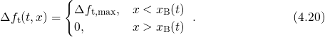
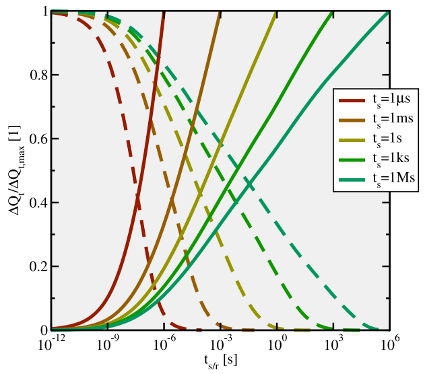
4.2.3 Time Behavior during Stress
In the following, the ETM will be tested whether it is consistent with the
experimental findings presented in Section 1.4. For this model evaluation, the
temporal behavior during the stress phase is the most essential criterion. It is
depicted in Fig. 4.8 as the evolution of trapped charges  and the threshold
voltage shift
and the threshold
voltage shift  . The former reveals a logarithmic time behavior, which
is preserved for a large time range and by far exceeds the measurement
window ranging from
. The former reveals a logarithmic time behavior, which
is preserved for a large time range and by far exceeds the measurement
window ranging from  to
to  . Recall that the behavior of one defect is
described by the rate equation (4.6), which has the form of an ordinary
first-order differential equation (4.1). It has been pointed out in Section 4.1
that the change in the occupancy
. Recall that the behavior of one defect is
described by the rate equation (4.6), which has the form of an ordinary
first-order differential equation (4.1). It has been pointed out in Section 4.1
that the change in the occupancy  is given by the dominating time
constants in the exponential term of equation (4.2). In the hole trapping
region (cf. Fig. 4.3),
is given by the dominating time
constants in the exponential term of equation (4.2). In the hole trapping
region (cf. Fig. 4.3),  holds. Then equation (4.2) simplifies to
Assuming a rectangular tunneling barrier for the WKB factor, one obtains
using the definitions and The exponential term on the right-hand side of equation (4.16) is characterized by a
sharp drop at which suggests the following approximation The sharp drop at  represents a border between defects which ‘already
have’ and ‘still do not have’ captured holes from the substrate until the
time
represents a border between defects which ‘already
have’ and ‘still do not have’ captured holes from the substrate until the
time  . This border moves away from the substrate towards deep into the
dielectric as time progresses (see Fig. 4.9). Its shift follows a time logarithmic
law according to equation (4.19) and results in straight lines in
. This border moves away from the substrate towards deep into the
dielectric as time progresses (see Fig. 4.9). Its shift follows a time logarithmic
law according to equation (4.19) and results in straight lines in  of
Fig. 4.8. When the border arrives at the gate, hole trapping stops, which
becomes visible as a saturation in
of
Fig. 4.8. When the border arrives at the gate, hole trapping stops, which
becomes visible as a saturation in  and
and  . According to
the charge sheet approximation, charges more distant from the substrate
oxide interface make a smaller contribution to
. According to
the charge sheet approximation, charges more distant from the substrate
oxide interface make a smaller contribution to  due to their smaller
weighting factors
due to their smaller
weighting factors  in equation (3.25). This yields the curvature seen
in
in equation (3.25). This yields the curvature seen
in  plots of Fig. 4.8. However, the resulting curves still roughly
follow a logarithmic time behavior. When disregarding the oxide field and
temperature dependence for the time being, this fact might be misinterpreted as
an agreement with the experimentally observed logarithmic time behavior
(1.8).
plots of Fig. 4.8. However, the resulting curves still roughly
follow a logarithmic time behavior. When disregarding the oxide field and
temperature dependence for the time being, this fact might be misinterpreted as
an agreement with the experimentally observed logarithmic time behavior
(1.8).
4.2.4 Time Range of Trapping
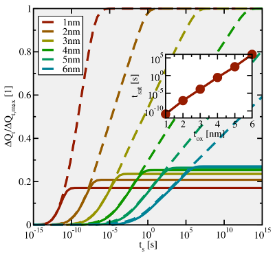
The simulations in Fig. 4.8 reveal that hole trapping sets in around  and lasts
over approximately 15 decades. In this context one should consider that the electrical
characterization methods used in NBTI have a limited time resolution of about
and lasts
over approximately 15 decades. In this context one should consider that the electrical
characterization methods used in NBTI have a limited time resolution of about  .
Therefore, they can only assess the accumulated degradation within a small
measurement window while a large part of the real degradation is invisible in the
experimental data. However, note that despite the wide time range, hole trapping is
limited to a few seconds in a
.
Therefore, they can only assess the accumulated degradation within a small
measurement window while a large part of the real degradation is invisible in the
experimental data. However, note that despite the wide time range, hole trapping is
limited to a few seconds in a  thick device (cf. Fig. 4.10). By contrast, no sign
of saturation has been experimentally observed in the stress phase of NBTI so
far.
thick device (cf. Fig. 4.10). By contrast, no sign
of saturation has been experimentally observed in the stress phase of NBTI so
far.
4.2.5 Oxide Field Dependence
The simulated curves in Fig. 4.8 have the same shape irrespective of the applied gate
bias and can be made overlap by multiplying them with appropriate scaling factors
 . According to measurement data,
  should follow a quadratic
field dependence up to approximately
should follow a quadratic
field dependence up to approximately  . However, the required scaling
factors do not show the correct tendency. Recall that only defects energetically
shifted above
. However, the required scaling
factors do not show the correct tendency. Recall that only defects energetically
shifted above  are capable of capturing holes. Therefore, the amount of
trapped charges per unit time is determined by the difference between
are capable of capturing holes. Therefore, the amount of
trapped charges per unit time is determined by the difference between  and
and
 before and during the application of the stress voltage. The relative
shift of these both energies is directly related to the surface potential
before and during the application of the stress voltage. The relative
shift of these both energies is directly related to the surface potential  according to equation (3.9). The simulations in Fig. 4.11 demonstrate that
  follows a nearly linear behavior over a wide range of the electric fields. As a
result, one obtains a linear dependence for
follows a nearly linear behavior over a wide range of the electric fields. As a
result, one obtains a linear dependence for  in the NBTI region
(indicated in Fig. 4.11), opposed to the quadratic field-acceleration observed in
experiments.
in the NBTI region
(indicated in Fig. 4.11), opposed to the quadratic field-acceleration observed in
experiments.
4.2.6 Time Behavior during Relaxation
In the simulated relaxation data in Fig. 4.12, the degradation returns back to its
pre-stress value, meaning that all defects charged during the stress phase also take
part in the recovery phase via hole emission. In these simulations it has been
presumed that the trapped holes can only tunneling back to the substrate. However
in devices with a small oxide thickness, the trapped charges can in principle be
emitted to the poly-gate contact. This case will be addressed in detail in
Section 4.2.8.
The simulations in Fig. 4.12 exhibit a logarithmic time behavior as
observed in experiments (see Section 1.4). As for the stress phase, hole
tunneling is determined by the WKB factor so that the tunneling times
increase exponentially with larger  . This gives rise to a tunneling
electron
front, which starts out from the substrate and continues deep into the dielectric as
illustrated in Fig. 4.13. The annihilation of trapped holes becomes visible as
straight lines in Fig. 4.12, consistent with the experimental findings for
the recovery phase. Against intuition, devices stressed at a higher gate bias
recover faster. This can be traced back to the fact that spatially deeper traps
have a reduced tunneling barrier when they are shifted down in the band
energy diagram during relaxation (see Fig. 4.14). The above behavior has not
been observed in measurements. This deviation from experimental data
could, in principle, also originate from an additional permanent or slowly
recovering component which is not accounted for in the present simulations.
As compared to the stress phase, the time span for the relaxation phase is
shortened for higher gate biases so that the recovery already ends before
. This gives rise to a tunneling
electron
front, which starts out from the substrate and continues deep into the dielectric as
illustrated in Fig. 4.13. The annihilation of trapped holes becomes visible as
straight lines in Fig. 4.12, consistent with the experimental findings for
the recovery phase. Against intuition, devices stressed at a higher gate bias
recover faster. This can be traced back to the fact that spatially deeper traps
have a reduced tunneling barrier when they are shifted down in the band
energy diagram during relaxation (see Fig. 4.14). The above behavior has not
been observed in measurements. This deviation from experimental data
could, in principle, also originate from an additional permanent or slowly
recovering component which is not accounted for in the present simulations.
As compared to the stress phase, the time span for the relaxation phase is
shortened for higher gate biases so that the recovery already ends before
 .
.
A remarkable peculiarity of NBTI is the the asymmetry in the slopes during stress
( ) and relaxation (
 ). It is related to the fact that
the recovery phase exceeds the duration of the stress phase by a couple
of decades. However, the ETM (see Fig. 4.15) predicts that the recovery
proceeds at equal pace or even faster than the degradation during stress
does. This is due to the fact that traps charged with
). It is related to the fact that
the recovery phase exceeds the duration of the stress phase by a couple
of decades. However, the ETM (see Fig. 4.15) predicts that the recovery
proceeds at equal pace or even faster than the degradation during stress
does. This is due to the fact that traps charged with  during stress
emit their holes with approximately the same time constants
during stress
emit their holes with approximately the same time constants  during
recovery.
during
recovery.
4.2.7 Investigation of the Temperature Dependence using a Quantum Refinement
Another important issue concern the temperature dependence of the ETM. Recall
that the experimental data exhibit an increased degradation at higher temperatures,
which was thought to go hand in hand with an enhanced ‘total’ hole concentration
 .
However, the simulations in Fig. 4.16 reveal an inverse tendency for the ETM. The
discrepancy might be attributed to a shift of the hole centroid into the substrate and
an associated reduction in the ‘interfacial’ hole concentration
.
However, the simulations in Fig. 4.16 reveal an inverse tendency for the ETM. The
discrepancy might be attributed to a shift of the hole centroid into the substrate and
an associated reduction in the ‘interfacial’ hole concentration  (see insert of
Fig. 4.16) for higher temperatures. In the band diagram, this is associated with a rise
of
(see insert of
Fig. 4.16) for higher temperatures. In the band diagram, this is associated with a rise
of  towards the center of the substrate bandgap and thus away from
  . The
relative position of
. The
relative position of  and
and  at the interface is the quantity which enters the
calculation of the tunneling rates (2.46) and yields a reduction in the amount of hole
trapping for higher temperatures. In a quantum mechanical treatment, the substrate
holes are described by channel wavefunctions, which are spread over the
whole channel region and penetrate deep into the dielectric. Tunneling and
thus charge trapping are eventually induced by the overlap of the hole and
trap wavefunctions. The ETM must be refined in order to account for the
quantum mechanical nature of the confined charge carriers in the channel.
Again equation (2.34) is taken as a starting point in the following derivation.
at the interface is the quantity which enters the
calculation of the tunneling rates (2.46) and yields a reduction in the amount of hole
trapping for higher temperatures. In a quantum mechanical treatment, the substrate
holes are described by channel wavefunctions, which are spread over the
whole channel region and penetrate deep into the dielectric. Tunneling and
thus charge trapping are eventually induced by the overlap of the hole and
trap wavefunctions. The ETM must be refined in order to account for the
quantum mechanical nature of the confined charge carriers in the channel.
Again equation (2.34) is taken as a starting point in the following derivation.

Here,  stands for the initial states. The sum over these states is split into
components parallel and perpendicular to the semiconductor-oxide interface, where
the charge carriers are confined in the latter direction. As derived in the
Appendix A.4, the number of states in an one-dimensional confined electron gas is
stands for the initial states. The sum over these states is split into
components parallel and perpendicular to the semiconductor-oxide interface, where
the charge carriers are confined in the latter direction. As derived in the
Appendix A.4, the number of states in an one-dimensional confined electron gas is
 denote the quantum numbers and
  the respective
eigenstates of the confined states in the conduction or the valence band,
respectively. Note that the integrals run from the first confined eigenstate
the respective
eigenstates of the confined states in the conduction or the valence band,
respectively. Note that the integrals run from the first confined eigenstate
 or
or  since they are located closest to the conduction or valence
band edges, respectively. Using (4.22), the rate (4.21) can be rewritten as
Due to the
since they are located closest to the conduction or valence
band edges, respectively. Using (4.22), the rate (4.21) can be rewritten as
Due to the  -function, the right-hand side of equation (4.22) can be simplified to
The refined variant of the ETM shows an increase in the total hole concentration
 (see inset of Fig. 4.17), which would suggest an increased degradation for
higher temperatures. Contrary to this ad hoc hypothesis, the simulations in Fig. 4.17
yield a reduced degradation, which is still in contrast to the experimental
observations (see Section 1.4). Actually, not the change in the hole concentration —
may it be
(see inset of Fig. 4.17), which would suggest an increased degradation for
higher temperatures. Contrary to this ad hoc hypothesis, the simulations in Fig. 4.17
yield a reduced degradation, which is still in contrast to the experimental
observations (see Section 1.4). Actually, not the change in the hole concentration —
may it be  or
or  — causes the inverse trend but the shift of
  relative to
 . From a statistical point of view, traps and band states at an energy
  will
equilibrate, meaning that their occupancies
will
equilibrate, meaning that their occupancies  and
and  will equalize. For higher
temperatures, the raise of
will equalize. For higher
temperatures, the raise of  in the band diagram implies a reduction of
  and in
consequence
and in
consequence  , which is related to the amount of trapped charges. It is important
to note here that the density of states only affects the rates but not the equilibrium
trap occupancies. In conclusion, the inverse temperature dependence cannot
be ascribed to the deficiency of the classical variant of the ETM but it is
inherent to elastic tunneling itself. Furthermore, the curves in Fig. 4.17 are
shifted approximately two decades towards earlier times compared to the
classical variant, which worsens the problem of the early saturation during
stress.
, which is related to the amount of trapped charges. It is important
to note here that the density of states only affects the rates but not the equilibrium
trap occupancies. In conclusion, the inverse temperature dependence cannot
be ascribed to the deficiency of the classical variant of the ETM but it is
inherent to elastic tunneling itself. Furthermore, the curves in Fig. 4.17 are
shifted approximately two decades towards earlier times compared to the
classical variant, which worsens the problem of the early saturation during
stress.
4.2.8 Charge Injection from the Gate
So far, the existing description of charge trapping has been restricted to
charge injection from the substrate. In device structures with thicker gate
dielectrics, the large tunneling distances from the gate towards the defects are
associated with small rates so that the presence of the gate contact as a
source or sink of charge carriers could be neglected. As the oxide thickness
of modern semiconductor devices has entered the nanometer range, this
assumption has lost its justification. Therefore, the ETM needs to be extended
by charge carrier injection from the gate. As illustrated in Fig. 4.18, this
can be achieved by introducing additional terms into the rates equation:

The subscripts  and
and  refer to quantities from the substrate or the poly-gate,
respectively. The simulations presented in Fig. 4.19 underline the importance of the
gate contact when thin dielectrics are considered. Recall that tunneling in the
conventional ETM can be envisaged as a tunneling hole front that starts at the
substrate interface and continues towards the gate. Traps located in the second half
of the dielectric are located closer to the gate and thus have shorter tunneling
distances to the gate. For these traps, electron injection from the gate outbalances
hole trapping from the substrate. Hence, the presence of the gate interface establishes
a spatial border to the penetrating hole front. When this border is reached, the
tunneling hole front stops, which causes an even earlier saturation during the stress
phase. At this point it is important to note that, depending on the spatial and
energetical distribution of traps, the band bending in the gate can also trigger
electron injection from the gate. A comparison of both models is presented in
Fig. 4.19. One may notice that the timescale for trapping is dramatically
reduced in the case of the extended ETM. For devices with relatively thick
gate dielectric of
refer to quantities from the substrate or the poly-gate,
respectively. The simulations presented in Fig. 4.19 underline the importance of the
gate contact when thin dielectrics are considered. Recall that tunneling in the
conventional ETM can be envisaged as a tunneling hole front that starts at the
substrate interface and continues towards the gate. Traps located in the second half
of the dielectric are located closer to the gate and thus have shorter tunneling
distances to the gate. For these traps, electron injection from the gate outbalances
hole trapping from the substrate. Hence, the presence of the gate interface establishes
a spatial border to the penetrating hole front. When this border is reached, the
tunneling hole front stops, which causes an even earlier saturation during the stress
phase. At this point it is important to note that, depending on the spatial and
energetical distribution of traps, the band bending in the gate can also trigger
electron injection from the gate. A comparison of both models is presented in
Fig. 4.19. One may notice that the timescale for trapping is dramatically
reduced in the case of the extended ETM. For devices with relatively thick
gate dielectric of  , the saturation sets in before
  . In technologically
more relevant device structures with a gate dielectrics thinner than
. In technologically
more relevant device structures with a gate dielectrics thinner than  ,
the degradation due to hole trapping ends before
,
the degradation due to hole trapping ends before  and would even be
not assessable with ultra-fast MSM measurements[27]. The fact that only
traps with short tunneling times participate during the stress phase is also
reflected in a fast removal of trapped charges during the relaxation phase.
The complete removal of positive charges during the relaxation phase is
achieved within approximately the same timescales than hole trapping during
stress. By contrast, the relaxation seen in experiments is often described as a
long-lasting process, which exceeds
and would even be
not assessable with ultra-fast MSM measurements[27]. The fact that only
traps with short tunneling times participate during the stress phase is also
reflected in a fast removal of trapped charges during the relaxation phase.
The complete removal of positive charges during the relaxation phase is
achieved within approximately the same timescales than hole trapping during
stress. By contrast, the relaxation seen in experiments is often described as a
long-lasting process, which exceeds  . More importantly, hole trapping is
reduced below five decades for oxide thicknesses below
. More importantly, hole trapping is
reduced below five decades for oxide thicknesses below  while the eMSM
data on a
while the eMSM
data on a  thick device (see Fig. 1.4) show at least seven decades.
4.2.9 Width of the Trap Band
Up to this point, only broad distributions of trap levels have been addressed.
However, it is speculated that some high- dielectrics have a crystalline
structure[166], which is characterized by small temperature-induced variations of
bond distances and angles. These lattice distortions yield a small spreading of defect
levels, seen as a small trap band in Fig. 4.20. In Fig. 4.20, the time evolution of
dielectrics have a crystalline
structure[166], which is characterized by small temperature-induced variations of
bond distances and angles. These lattice distortions yield a small spreading of defect
levels, seen as a small trap band in Fig. 4.20. In Fig. 4.20, the time evolution of
 is plotted for a narrow distribution of defect levels. During stress, the onset of
hole trapping is shifted towards earlier times for increasing gate voltages. This
behavior can be traced back to different defects involved in charge trapping at
different
is plotted for a narrow distribution of defect levels. During stress, the onset of
hole trapping is shifted towards earlier times for increasing gate voltages. This
behavior can be traced back to different defects involved in charge trapping at
different  (see Fig. 4.21). As the gate bias is increased, defects located closer to
the substrate interface are moved into the region around the Fermi level. Due to
their reduced tunneling distances, they feature shorter trapping times and
therefore give rise to an earlier onset in the
(see Fig. 4.21). As the gate bias is increased, defects located closer to
the substrate interface are moved into the region around the Fermi level. Due to
their reduced tunneling distances, they feature shorter trapping times and
therefore give rise to an earlier onset in the  curves. Since the defects
in the active trapping region are spatially concentrated to a small region,
their corresponding tunneling distances are limited to a small range. Thus
the distribution of trapping times is sharply peaked, which becomes visible
as sudden jumps in the
curves. Since the defects
in the active trapping region are spatially concentrated to a small region,
their corresponding tunneling distances are limited to a small range. Thus
the distribution of trapping times is sharply peaked, which becomes visible
as sudden jumps in the  curves of Fig. 4.20. The shape of these
curves is in stark contrast to the wide range of timescales usually involved in
NBTI.
curves of Fig. 4.20. The shape of these
curves is in stark contrast to the wide range of timescales usually involved in
NBTI.


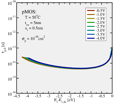
 ) and emission times (
 ) for two
different temperatures as a function of the trap level
) for two
different temperatures as a function of the trap level  . The simulated device
is subject to heavy stress conditions, at which tunneling ‘through’ the dielectric
actually play a crucial role and should be taken into account. Nevertheless,
. The simulated device
is subject to heavy stress conditions, at which tunneling ‘through’ the dielectric
actually play a crucial role and should be taken into account. Nevertheless,  is set to a high gate voltage for illustration purposes only. The Fermi-Dirac
distribution predicts a decrease in
is set to a high gate voltage for illustration purposes only. The Fermi-Dirac
distribution predicts a decrease in  above
above  , which leads to exponentially
rising
, which leads to exponentially
rising  . Analogously,
  decays and
  rises below the
  . As a
result,
. As a
result,  is larger than
  in the region above the
  so that hole
trapping can occur there. By contrast, hole trapping is inhibited below
so that hole
trapping can occur there. By contrast, hole trapping is inhibited below  since
since  . For higher temperatures, the exponential decay becomes
weaker, which is reflected in smaller slopes of the
. For higher temperatures, the exponential decay becomes
weaker, which is reflected in smaller slopes of the  and
and  .
. 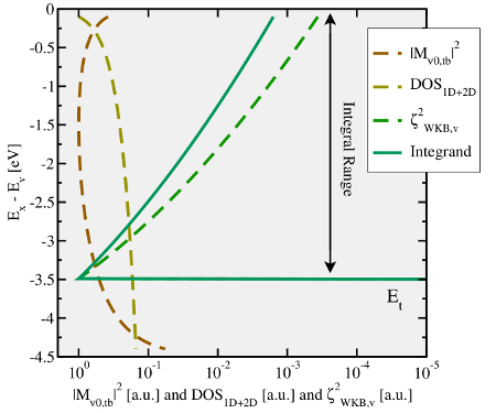
 ,
,  , the
, the
 , and their product for flat band conditions. For better visibility,
all functions are normalized to their maximal values. While
, and their product for flat band conditions. For better visibility,
all functions are normalized to their maximal values. While  and
and  remain within one order of magnitude, the WKB factor
drops significantly. Since only the product of the three quantities enters the
integrand of the rate equation (
remain within one order of magnitude, the WKB factor
drops significantly. Since only the product of the three quantities enters the
integrand of the rate equation ( .
.
 as a function of the trap level for different
gate biases. Note that
as a function of the trap level for different
gate biases. Note that  remains within one or two orders of magnitude.
The peaks close to
remains within one or two orders of magnitude.
The peaks close to  can be traced back to a small kinetic energy of the holes
within a classical picture. Quantum mechanically, the amplitude of the channel
wavefunction at the interface is reduced for smaller charge carrier energies. This
results in a decreased overlap of the wavefunction in the matrix element, a
smaller tunneling probability, and ultimately in larger
can be traced back to a small kinetic energy of the holes
within a classical picture. Quantum mechanically, the amplitude of the channel
wavefunction at the interface is reduced for smaller charge carrier energies. This
results in a decreased overlap of the wavefunction in the matrix element, a
smaller tunneling probability, and ultimately in larger  close to the band
edges.
close to the band
edges.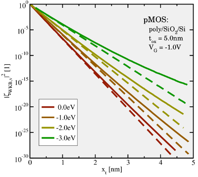
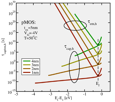
 ) and emission
(
) and emission
( ) times constants on the trap depths. The more distant the traps
are located from the interface, the larger become
) times constants on the trap depths. The more distant the traps
are located from the interface, the larger become  and
and  .
This can be ascribed to the properties of the WKB factor, which decreases
exponentially with the spatial depth of traps. Hence, the tunneling rates are
reduced but the tunneling times are increased for deeper traps. Note that the
crossing between
.
This can be ascribed to the properties of the WKB factor, which decreases
exponentially with the spatial depth of traps. Hence, the tunneling rates are
reduced but the tunneling times are increased for deeper traps. Note that the
crossing between  and
and  always coincides with
  , irrespectively of
the tunneling distance. As a consequence, the energetical border to the trapping
region does not vary with the trap depth.
, irrespectively of
the tunneling distance. As a consequence, the energetical border to the trapping
region does not vary with the trap depth.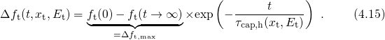


 as a function
of stress time for different gate biases (
as a function
of stress time for different gate biases ( ). Charge trapping occurs
over up to approximately 15 decades and shows a logarithmic time dependence.
The slopes in the plot increase linearly with the oxide field, which cannot
be reconciled with the quadratic field dependence obtained from experiments.
). Charge trapping occurs
over up to approximately 15 decades and shows a logarithmic time dependence.
The slopes in the plot increase linearly with the oxide field, which cannot
be reconciled with the quadratic field dependence obtained from experiments.
 for different gate
biases. The resulting curves roughly approximate a logarithmic time dependence
in a small experimental window from
for different gate
biases. The resulting curves roughly approximate a logarithmic time dependence
in a small experimental window from  to
to  .
.
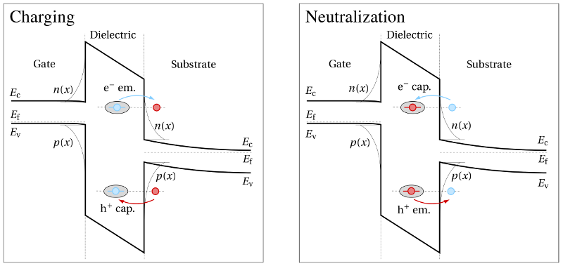
 ).
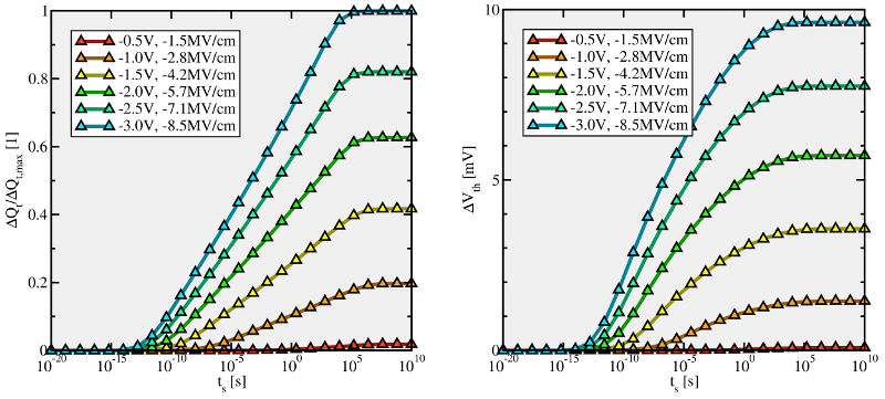
Single traps are represented by the small circles located in the lower part of the
oxide bandgap, where the occupied and the empty states are depicted as purple
and white filled circles, respectively. The hole occupation of traps in the band
diagram is recorded for a series of stress times and demonstrates the filling of
traps with time. One can recognize a tunneling hole front, which starts from
the substrate (right) and penetrates deep into the dielectric (towards the left).
For demonstration purposes, the simulations were performed with the upper
edge of the trap band shifted slightly above the substrate valence band. Note
that traps located above the Fermi level do not have captured holes. This is
due to the fact that these traps are energetically located within the substrate
bandgap and thus have no corresponding energy level which can serve as a hole
source in a tunneling process. Furthermore, hole trapping from the poly-gate
has been neglected in these simulations but this aspect will be addressed later
in Section
).
Single traps are represented by the small circles located in the lower part of the
oxide bandgap, where the occupied and the empty states are depicted as purple
and white filled circles, respectively. The hole occupation of traps in the band
diagram is recorded for a series of stress times and demonstrates the filling of
traps with time. One can recognize a tunneling hole front, which starts from
the substrate (right) and penetrates deep into the dielectric (towards the left).
For demonstration purposes, the simulations were performed with the upper
edge of the trap band shifted slightly above the substrate valence band. Note
that traps located above the Fermi level do not have captured holes. This is
due to the fact that these traps are energetically located within the substrate
bandgap and thus have no corresponding energy level which can serve as a hole
source in a tunneling process. Furthermore, hole trapping from the poly-gate
has been neglected in these simulations but this aspect will be addressed later
in Section 
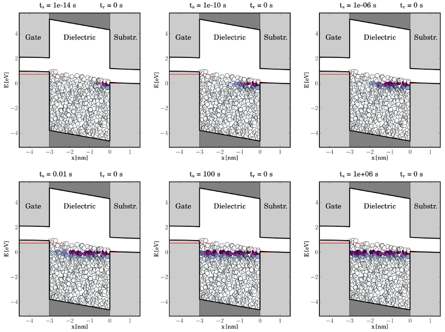
 ,
,  ). For comparison with Section
  below the substrate valence
band edge in this simulation. One can observe an early saturation for devices
with an oxide thickness equal or smaller than
below the substrate valence
band edge in this simulation. One can observe an early saturation for devices
with an oxide thickness equal or smaller than  , not seen in experiments.
The inset shows that the time point of saturation is shifted out of the
measurement window for devices with an oxide thickness notably exceeding a
value of
, not seen in experiments.
The inset shows that the time point of saturation is shifted out of the
measurement window for devices with an oxide thickness notably exceeding a
value of  .
. 
 versus the applied gate bias and
the oxide field for the simulated pMOSFET (
versus the applied gate bias and
the oxide field for the simulated pMOSFET ( ). This quantity is
proportional to the scaling factor
). This quantity is
proportional to the scaling factor  in the simulated curves of Fig.
  shows a nearly linear dependence on the oxide field.
 curve for heavier stress conditions, which shifts
the end of the relaxation phase below
curve for heavier stress conditions, which shifts
the end of the relaxation phase below  .
.
 ,
,
 ) for different stress times. Each pair of curves is normalized to the
last stress value. Note that both curves approximately cover the same number of
decades, which is in disagreement with the experimentally obtained asymmetry
in the slopes during the stress and the relaxation phase.
) for different stress times. Each pair of curves is normalized to the
last stress value. Note that both curves approximately cover the same number of
decades, which is in disagreement with the experimentally obtained asymmetry
in the slopes during the stress and the relaxation phase.
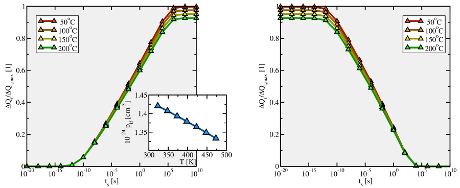
 . Surprisingly, the classical simulations predict a decrease in the
amount of trapped holes for higher temperatures. This seems to be related to
the reduction in the interfacial hole concentration
. Surprisingly, the classical simulations predict a decrease in the
amount of trapped holes for higher temperatures. This seems to be related to
the reduction in the interfacial hole concentration  shown in the insert of
the left plot.
shown in the insert of
the left plot.
 (see the insert of the
left plot) would suggest an increased hole trapping for higher temperatures. In
comparison to the classical variant, a shift of the whole set of curves towards
earlier times is observed.
(see the insert of the
left plot) would suggest an increased hole trapping for higher temperatures. In
comparison to the classical variant, a shift of the whole set of curves towards
earlier times is observed.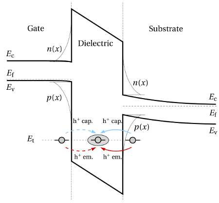
 ,
,  ). It is
noted that the uppermost trap level is located
). It is
noted that the uppermost trap level is located  below the substrate
valence band edge in this simulation. In the case of the extended ETM, one can
recognize an early saturation, which reflects the stopping of the hole front in
the dielectric. As pointed out in the inset, this time point of saturation is moved
towards an earlier time, which may lie within typical measurement windows for
NBTI (ranging from
below the substrate
valence band edge in this simulation. In the case of the extended ETM, one can
recognize an early saturation, which reflects the stopping of the hole front in
the dielectric. As pointed out in the inset, this time point of saturation is moved
towards an earlier time, which may lie within typical measurement windows for
NBTI (ranging from  to
to  ). One should keep in mind that only devices
with an oxide thickness thicker than
). One should keep in mind that only devices
with an oxide thickness thicker than  show a logarithmic time behavior
beyond
show a logarithmic time behavior
beyond  , which corresponds to the largest investigated stress times.
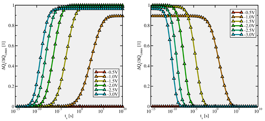
 (
( ) for
stress (left) and relaxation (right) presuming a narrow distribution of defect
levels (
) for
stress (left) and relaxation (right) presuming a narrow distribution of defect
levels ( ) centered around
  below the substrate valence band
edge. For this assumption, the ETM predicts short jumps or drops in
below the substrate valence band
edge. For this assumption, the ETM predicts short jumps or drops in  for both phases, which are limited to only a very few decades. This cannot be
reconciled with NBTI data with a relaxation phase that spans over 10 decades.
In the case of
for both phases, which are limited to only a very few decades. This cannot be
reconciled with NBTI data with a relaxation phase that spans over 10 decades.
In the case of  , the defect levels are not moved into the region around
the Fermi level so that no trapping can occur.
, the defect levels are not moved into the region around
the Fermi level so that no trapping can occur.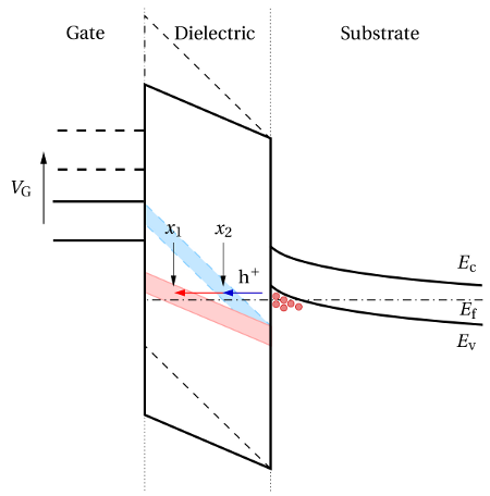
 ) where traps with smaller tunneling time constants (
 ) are
situated. This leads to an earlier onset of charge trapping for higher gate
voltages.
) are
situated. This leads to an earlier onset of charge trapping for higher gate
voltages.